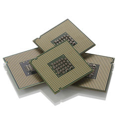
GS8161Z36DGD-200V
SRAM Chip Sync Quad 1.8V/2.5V 18M-Bit 512K x 36 6.5ns/3ns 165-Pin FBGA
- RoHS 10 Compliant
- Tariff Charges
The GS8161Z36 is an 18Mbit Synchronous Static SRAM. GSI's NBT SRAMs, like ZBT, NtRAM, NoBL or other pipelined read/double late write or flow through read/single late write SRAMs, allow utilization of all available bus bandwidth by eliminating the need to insert deselect cycles when the device is switched from read to write cycles. Because it is a synchronous device, address, data inputs, and read/ write control inputs are captured on the rising edge of the input clock. Burst order control (LBO) must be tied to a power rail for proper operation. Asynchronous inputs include the Sleep mode enable, ZZ and Output Enable. Output Enable can be used to override the synchronous control of the output drivers and turn the RAM's output drivers off at any time. Write cycles are internally self-timed and initiated by the rising edge of the clock input. This feature eliminates complex off chip write pulse generation required by asynchronous SRAMs and simplifies input signal timing. The GS8161Z36 may be configured by the user to operate in Pipeline or Flow Through mode. Operating as a pipelined synchronous device, in addition to the rising-edge-triggered registers that capture input signals, the device incorporates a rising-edge-triggered output register. For read cycles, pipelined SRAM output data is temporarily stored by the edge triggered output register during the access cycle and then released to the output drivers at the next rising edge of clock. The GS8161Z36 is implemented with GSI's high performance CMOS technology and is available in JEDEC-standard 100-pin TQFP and 165-bump FP-BGA packages.
- User-configurable Pipeline and Flow Through mode
- NBT (No Bus Turn Around) functionality allows zero wait read-write-read bus utilization
- Fully pin-compatible with both pipelined and flow through NtRAM™, NoBL™ and ZBT™ SRAMs
- IEEE 1149.1 JTAG-compatible Boundary Scan
- 2.5 V or 3.3 V +10%/–10% core power supply
- LBO pin for Linear or Interleave Burst mode
- Pin-compatible with 2M, 4M, and 8M devices
- Byte write operation (9-bit Bytes)
- 3 chip enable signals for easy depth expansion
- ZZ pin for automatic power-down
- JEDEC-standard 100-lead TQFP and 165-bump FP-BGA packages
Technical Attributes
Find Similar Parts
| Description | Value | |
|---|---|---|
| 19 Bit | ||
| Flow-Through|Pipelined | ||
| 200 MHz | ||
| SDR | ||
| 18 Mbit | ||
| 210@Flow-Through|205@Pipelined mA | ||
| 2, 2.7 V | ||
| 6.5@Flow-Through|3@Pipelined ns | ||
| 18 Mbit | ||
| 1.7, 2.3 V | ||
| Surface Mount | ||
| 165 | ||
| 36 Bit | ||
| 36 Bit | ||
| 4 | ||
| 512 kWords | ||
| 0 to 85 °C | ||
| 85 °C | ||
| 0 °C | ||
| 165FBGA | ||
| 165 | ||
| 15 x 13 x 0.94 mm | ||
| No | ||
| Commercial | ||
| FBGA | ||
| 2.7, 2.7 V | ||
| 2.3, 2.3 V | ||
| 2.5, 2.5 V | ||
| Synchronous | ||
| 1.8, 2.5 V |
ECCN / UNSPSC / COO
| Description | Value |
|---|---|
| Country of Origin: | RECOVERY FEE |
| ECCN: | 3A991.B.2.B |
| HTSN: | 8542320041 |
| Schedule B: | 8542320040 |
