
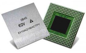
EV10AQ190AVTPY
Analog to Digital Converter, 10 bit, Pipelined, 5 GSPS, Differential, LVDS, SPI, 4.75 V to 5.05 V, 380 Pins, E-BGA
-
 RoHS 10 Compliant
 -
 Tariff Charges
The Quad ADC is made up of four 10-bit ADC cores which can be considered independently (fourchannel mode) or grouped by 2 x 2 cores (two-channel mode with the ADCs interleaved two by two) or one-channel mode (where all four ADCs are all interleaved together).
All four ADCs are clocked by the same external input clock signal and controlled via an industry standard SPI (Serial Peripheral Interface). An analog multiplexer (cross point switch) is used to select the analog inputs depending on the mode the Quad ADC is used in.
The clock circuit is common to all four ADCs. This block receives an external 2.5 GHz clock (maximum frequency) and preferably a low jitter sinewave signal.
- Quad ADC with 10-bit Resolution Using e2v Proprietary Analog Input Cross-point Switch 1.25 Gsps Sampling Rate in Four-channel Mode 2.5 Gsps Sampling Rate in Two-channel Mode 5 Gsps Sampling Rate in One-channel Mode Built-in four-by-four Cross Point Switch
- Single 2.5 GHz Differential Symmetrical Input Clock
- 500 mVpp Analog Input (Differential AC or DC Coupled)
- ADC Master Reset (LVDS)
- Double Data Rate Output Protocol
- LVDS Output Format
- Digital Interface (SPI) with Reset Signal: Channel Mode Selection Selectable Bandwidth (Two Available Settings) Gain Control Offset Control Phase Control Standby Mode (Full or Partial) Binary or Gray Coding Selection Test Modes (Ramp, Flashing)
- Power Supplies: 3.3V and 1.8V (Outputs)
- Reduced Clock Induced Transients on Power Supply Pins due to BiCMOS Silicon Technology
- Power Dissipation: 1.4W per Channel
- EBGA380 Package (RoHS, 1.27 mm Pitch)
Technical Attributes
Find Similar Parts
| Description | Value | |
|---|---|---|
| Pipelined | ||
| E-BGA | ||
| Surface Mount | ||
| Differential | ||
| LVDS, SPI | ||
| 4 | ||
| 380 | ||
| 5.5, 2.8 V | ||
| 110 °C | ||
| -40 °C | ||
| Quad 10-Bit Pipelined ADCs | ||
| 10 Bits | ||
| 5 Gsps | ||
| 5.05 V | ||
| 4.75 V |
ECCN / UNSPSC / COO
| Description | Value |
|---|---|
| Country of Origin: | RECOVERY FEE |
| ECCN: | 3A001.A.5.A.2 |
| HTSN: | 8542390050 |
| Schedule B: | 8542390060 |