
9DML4493ANLGI
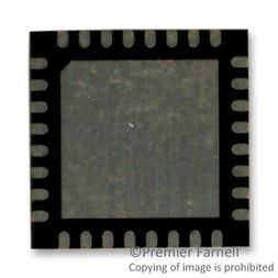
Clock Multiplexer, 4 Outputs, 1.71 V to 3.465 V, 32 Pins, VFQFPN-EP
Click image to enlarge
Manufacturer:Renesas Electronics
Product Category:
Clock & Timing, Clock Generators & Synthesizers
Avnet Manufacturer Part #: 9DML4493ANLGI
Secondary Manufacturer Part#: 9DML4493ANLGI
-
 RoHS 10 Compliant
 -
 Tariff Charges

9DML4493ANLGI is a 4:4 clock MUX for PCI express gen1–6. It can also operate as a dual 2-input, 2-output clock multiplexer. It has very low additive phase jitter and is suitable for all PCIe data rates. The device supports today's complex system power sequencing requirements with power down tolerant and flexible power sequencing features. Typical application includes servers storage, networking, high-performance computing, accelerators.
- 5 × 5mm 32-VFQFPN package
- Four differential inputs support LVPECL, LVDS, HCSL or LVCMOS reference clocks
- Accepts input frequency ranging from 1PPS to 350MHz, configured via pin straps no serial bus needed
- Spread-spectrum tolerant
- Glitch-free output enable pins for each output
- Additive phase jitter is 8fs RMS typ (PCIe Gen6 CC at 100MHz), 66fs RMS typ (12kHz–20MHz at 156.25M)
- Propagation delay is 1.2ns typical
- Supports common clocked (CC) and IR (SRIS, SRNS) timing architectures
- Voltage supply of 1.8V, 2.5V, or 3.3V
- Temperature range from -40°C to +85°C
Technical Attributes
Find Similar Parts
| Description | Value | |
|---|---|---|
| Clock Multiplexer | ||
| VFQFPN-EP | ||
| HCSL, LVCMOS, LVDS, LVPECL | ||
| 4 | ||
| 32 | ||
| 85 °C | ||
| -40 °C | ||
| LP-HCSL | ||
| 3.465 V | ||
| 1.71 V |
ECCN / UNSPSC / COO
| Description | Value |
|---|---|
| Country of Origin: | RECOVERY FEE |
| ECCN: | EAR99 |
| HTSN: | 8542390090 |
| Schedule B: | 8542390060 |
 Factory Lead Time: