
9DB633AGLFT
6-output 3.3 V PCIe Gen1-2-3 Zero Delay / Fanout Buffer
Click image to enlarge
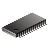
Manufacturer:Renesas Electronics
Product Category:
RF & Wireless, Other RF & Wireless
Avnet Manufacturer Part #: 9DB633AGLFT
Secondary Manufacturer Part#: 9DB633AGLFT
-
 RoHS 10 Compliant
 -
 Tariff Charges

The 9DB633 zero-delay buffer supports PCIe Gen3 requirements, while being backwards compatible to PCIe Gen2 and Gen1. The 9DB633 is driven by a differential SRC output pair from an IDT 932S421 or 932SQ420 or equivalent main clock generator. It attenuates jitter on the input clock and has a selectable PLL bandwidth to maximize performance in systems with or without Spread-Spectrum clocking. An SMBus interface allows control of the PLL bandwidth and bypass options, while 2 clock request (OE#) pins make the 9DB633 suitable for Express Card applications.
- OE# pins/Suitable for Express Card applications
- PLL or bypass mode/PLL can dejitter incoming clock
- Selectable PLL bandwidth/minimizes jitter peaking in downstream PLL's
- Spread Spectrum Compatible/tracks spreading input clock for low EMI
- SMBus Interface/unused outputs can be disabled
Technical Attributes
Find Similar Parts
| Description | Value | |
|---|---|---|
| Matte Tin | ||
| 260 °C | ||
| 110 MHz | ||
| 33 MHz | ||
| Surface Mount | ||
| MSL 1 - Unlimited | ||
| 1 | ||
| 3.3 V | ||
| 0 to 70 °C | ||
| 28TSSOP | ||
| 28 | ||
| 0.6500 | ||
| 0 | ||
| Commercial | ||
| Zero Delay PLL Clock Buffer |
ECCN / UNSPSC / COO
| Description | Value |
|---|---|
| Country of Origin: | RECOVERY FEE |
| ECCN: | EAR99 |
| HTSN: | 8542390090 |
| Schedule B: | 8542390060 |
 Factory Lead Time: