
8P34S1102NLGI8
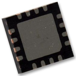
Clock Fanout Buffer, CML, LVDS, 1.2 GHz, 2 Outputs, 1.71V to 1.89V, VFQFN-16
-
 RoHS 10 Compliant
 -
 Tariff Charges

8P34S1102NLGI8 is a high-performance differential LVDS fanout buffer. The device is designed for the fanout of 1PPS signals or high-frequency, very low additive phase-noise clock and data signals. The 8P34S1102 supports fail-safe operation and is characterized to operate from a 1.8V or 2.5V power supply. Guaranteed output-to-output and part-to-part skew characteristics make the 8P34S1102 ideal for those clock distribution applications demanding well-defined performance and repeatability. One differential input and two low skew outputs are available. The integrated bias voltage reference enables easy interfacing of single-ended signals to the differential device input. The device is optimized for low power consumption and low additive phase noise.
- Two low skew, low additive jitter LVDS output pairs
- One differential clock input pair
- Differential CLK, nCLK pairs can accept the following differential input levels: LVDS, CML
- Maximum input clock frequency of 51.2GHz
- Output skew of 3ps (typical), propagation delay of 400ps (maximum)
- Low additive phase jitter, RMS; fREF = 156.25MHz, 10KHz–20MHz: 34fs (typical)
- Device current consumption (IDD) of 40mA typical: 1.8V, 50mA typical: 2.5V
- Available in 16 pin VFQFN package
- Ambient operating temperature range from -40°C to 85°C
- Supports PCI Express Gen 1-5
Technical Attributes
Find Similar Parts
| Description | Value | |
|---|---|---|
| Fanout Buffer | ||
| VFQFPN-EP | ||
| 1.5 GHz | ||
| CML, LVDS | ||
| 1 | ||
| 2 | ||
| 16 | ||
| 85 °C | ||
| -40 °C | ||
| LVDS | ||
| 8P34S1102 Series | ||
| 2.7 Vdc | ||
| 2.1 Vdc |
ECCN / UNSPSC / COO
| Description | Value |
|---|---|
| Country of Origin: | RECOVERY FEE |
| ECCN: | EAR99 |
| HTSN: | 8542390090 |
| Schedule B: | 8542390060 |
 Factory Lead Time: