
5PB1104CMGI
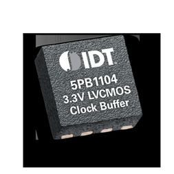
Clock Buffer, Fanout, 0 MHz to 200 MHz, 4 Outputs, 1.71 V to 3.465 V, 8 Pins, DFN
Click image to enlarge
Manufacturer:Renesas Electronics
Product Category:
Clock & Timing, Clock Buffers
Avnet Manufacturer Part #: 5PB1104CMGI
Secondary Manufacturer Part#: 5PB1104CMGI
-
 RoHS 10 Compliant
 -
 Tariff Charges

The 5PB1104 is a high-performance LVCMOS Clock Buffer Family. It has best-in-class Additive Phase Jitter of 50fsec RMS. There are five different fan-out variations, 1:2 to 1:10, available. The IDT5PB1104 also supports a synchronous glitch-free Output Enable function to eliminate any potential intermediate incorrect output clock cycles when enabling or disabling outputs. It comes in various packages and can operate from a 1.8V to 3.3V supply.
- High performance 1:2, 1:4, 1:6, 1:8, 1:10 LVCMOS clock buffer
- Very low pin-to-pin skew <50 ps
- Very low additive jitter <50 fs
- Supply voltage: 1.8V to 3.3V
- fMAX = 200MHz
- Integrated serial termination for 50ohm channel
- Packaged in 8-, 14-, 16-, 20-pin TSSOP and small DFN and QFN packages
- Extended (-40°C to +105°C) temperature range
Technical Attributes
Find Similar Parts
| Description | Value | |
|---|---|---|
| Fanout Buffer | ||
| 200 MHz | ||
| 0 MHz | ||
| LVCMOS | ||
| 1 | ||
| 4 | ||
| 8 | ||
| 85 °C | ||
| -40 °C | ||
| LVCMOS | ||
| 5PB11xx Series | ||
| 3.465 Vdc | ||
| 1.71 Vdc |
ECCN / UNSPSC / COO
| Description | Value |
|---|---|
| Country of Origin: | RECOVERY FEE |
| ECCN: | EAR99 |
| HTSN: | 8542390090 |
| Schedule B: | 8542390060 |
 Factory Lead Time: