
5P1103A000NLGI
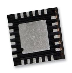
Programmable Fanout Buffer
-
 RoHS 10 Compliant
 -
 Tariff Charges

The 5P1103 is a programmable fanout buffer intended for high performance consumer, networking, industrial, computing, and data-communications applications. Configurations may be stored in on-chip One-Time Programmable (OTP) memory or changed using I²C interface. The outputs are generated from a single reference clock. The input reference can be crystal, external single-ended or differential clock. The reference clock can come from one of the two redundant clock inputs and is selected by CLKSEL pin. A glitchless manual switchover function allows one of the redundant clocks to be selected during normal operation. See reference clock input section for details. Two select pins allow up to 4 different configurations to be programmed and accessible using processor GPIOs or bootstrapping.
- Up to two high performance universal differential output pairs
- Low RMS additive phase jitter: 0.2ps
- Four banks of internal non-volatile in-system programmable or factory programmable OTP memory
- I²C serial programming interface
- One additional LVCMOS output clock
- I/O Standards:
- Single-ended I/Os: 1.8V to 3.3V LVCMOS
- Differential I/Os - LVPECL, LVDS and HCSL
- Individually selectable output voltage (1.8V, 2.5V, 3.3V) for each output pair
- Redundant clock inputs with manual switchover
- Programmable crystal load capacitance
- Individual output enable/disable
- Power-down mode
- 1.8V, 2.5V or 3.3V core VDDD, VDDA
- Available in 24-pin VFQFPN 4mm x 4mm package
- -40°Cto +85°C industrial temperature operation
Technical Attributes
Find Similar Parts
| Description | Value | |
|---|---|---|
| 24 | ||
| 85 °C | ||
| -40 °C | ||
| 3.465 V | ||
| 1.71 V |
ECCN / UNSPSC / COO
| Description | Value |
|---|---|
| Country of Origin: | RECOVERY FEE |
| ECCN: | EAR99 |
| HTSN: | 8542390090 |
| Schedule B: | 8542390060 |
 Factory Lead Time: