
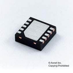
NCP51401MNTXG
3 Amp VTT Termination Regulator DDR1, DDR2, DDR3, LPDDR3, DDR4. ONSSPCLDO;
-
 RoHS 10 Compliant
 -
 Tariff Charges
The NCP51401 is a source/sink Double Data Rate (DDR) termination regulator specifically designed for low input voltage and low-noise systems where space is a key consideration. The NCP51401 maintains a fast transient response and only requires a minimum output capacitance of 20 F. The NCP51401 supports a remote sensing function and all power requirements for DDR VTT bus termination. The NCP51401 can also be used in low-power chipsets and graphics processor cores that require dynamically adjustable output voltages. he NCP51401 is available in the thermally-efficient DFN10 Exposed Pad package, and is rated both Green and Pb-free.
Input Voltage Rails: Supports 2.5 V, 3.3 V and 5 V Rails PVCC Voltage Range: 1.1 to 3.5 V Integrated Power MOSFETs Source and Sink Termination Regulator with Droop Compensation Fast Load-Transient Response PGOOD - Logic output pin to Monitor VTT Regulation EN - Logic input pin for Shutdown mode VRI - Reference Input Allows for Flexible Input Tracking Either Directly or Through Resistor Divider Remote Sensing (VTTS) Built-in Under Voltage Lockout and Over Current Limit Thermal Shutdown Small, Low-Profile 10-pin, 3x3 DFN Package These Devices are Pb-Free and are RoHS Compliant
Technical Attributes
Find Similar Parts
| Description | Value | |
|---|---|---|
| 5.5 V | ||
| DDR1, DDR2, DDR3, LPDDR3, DDR4, DDR2, DDR3 | ||
| 2.375 V | ||
| Surface Mount | ||
| 10 | ||
| -40 to 125 °C | ||
| 125 °C | ||
| -40 °C | ||
| 10 | ||
| 3 A | ||
| 3 A | ||
| DFN | ||
| 5.5 V | ||
| 2.375 V |
ECCN / UNSPSC / COO
| Description | Value |
|---|---|
| Country of Origin: | RECOVERY FEE |
| ECCN: | EAR99 |
| HTSN: | 8542390050 |
| Schedule B: | 8542390060 |