
NB6N14SMNG
Clock / Data Fanout Buffer, 1:4 AnyLevel™ Input, LVDS, 3.3 V
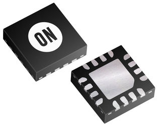
-
 RoHS 10 Compliant
 -
 Tariff Charges

The NB6N14SMNG is a 3.3V 1:4 AnyLevel differential input to LVDS fan-out buffer/translator in 16 pin QFN package. This differential 1:4 clock or data receiver and will accept AnyLevel differential input signals, LVPECL, CML or LVDS. These signals will be translated to LVDS and four identical copies of clock or data will be distributed, operating up to 2GHz or 2.5Gb/s, respectively. As such, the NB6N14S is ideal for SONET, GigE, fibre channel, backplane and other clock or data distribution applications. It has a wide input common mode range from GND + 50mV to VCC - 50mV. Combined with the 50 ohm internal termination resistors at the inputs, the NB6N14S is ideal for translating a variety of differential or single ended clock or data signals to 350mV typical LVDS output levels.
- Maximum input clock frequency 2GHz
- Maximum input data rate 2.5Gb/s
- 1ps maximum RMS clock jitter
- Typically 10ps data dependent jitter
- 380ps typical propagation delay
- 120ps typical rise and fall times
- Vref_ac reference output
- TIA/EIA - 644 compliant
- Functionally compatible with existing 3.3V LVEL, LVEP, EP and SG devices
Technical Attributes
Find Similar Parts
| Description | Value | |
|---|---|---|
| Fanout Buffer, Translator | ||
| QFN-EP | ||
| 2000(Min) MHz | ||
| 2 GHz | ||
| CML, LVCMOS, LVDS, LVPECL, LVTTL | ||
| 1 | ||
| 4 | ||
| 16 | ||
| 85 °C | ||
| -40 °C | ||
| LVDS | ||
| NB6N14S Series | ||
| 3.6 Vdc | ||
| 3 Vdc |
ECCN / UNSPSC / COO
| Description | Value |
|---|---|
| Country of Origin: | RECOVERY FEE |
| ECCN: | EAR99 |
| HTSN: | 8542390070 |
| Schedule B: | 8542390060 |
 Factory Lead Time: