
NB6N11SMNR2G
Clock / Data Fanout Buffer, 1:2 AnyLevel™ Input, LVDS, 3.3 V
-
 RoHS 10 Compliant
 -
 Tariff Charges

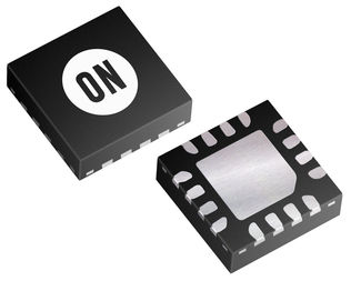
The NB6N11S is a differential 1:2 Clock or Data Receiver and will accept AnyLevelTM input signals: LVPECL, CML, LVCMOS, LVTTL, or LVDS. These signals will be translated to LVDS and two identical copies of Clock or Data will be distributed, operating up to 2.0 GHz or 2.5 Gb/s, respectively. As such, the NB6N11S is ideal for SONET, GigE, Fiber Channel, Backplane and other Clock or Data distribution applications. The NB6N11S has a wide input common mode range from GND + 50mV to VCC - 50 mV. Combined with the 50-ohm internal termination resistors at the inputs, the NB6N11S is ideal for translating a variety of differential or single-ended Clock or Data signals to 350 mV typical LVDS output levels. The NB6N11S is functionally equivalent to the EP11, LVEP11, SG11 or 7L11M devices and is offered in a small 3mm X 3mm 16-QFN package.
- Maximum Input Clock Frequency > 2.0 GHz
- Maximum Input Data Rate > 2.5 Gb/s
- 1 ps Maximum of RMS Clock Jitter
- Typically 10 ps of Data Dependent Jitter
- 380 ps Typical Propagation Delay
- 120 ps Typical Rise and Fall Times
- These devices are available in Pb-free package(s). Specifications herein
Technical Attributes
Find Similar Parts
| Description | Value | |
|---|---|---|
| Fanout Buffer, Translator | ||
| QFN-EP | ||
| 2 GHz | ||
| CML, LVCMOS, LVDS, LVPECL, LVTTL | ||
| 1 | ||
| 2 | ||
| 16 | ||
| 85 °C | ||
| -40 °C | ||
| LVDS | ||
| NB6N11S Series | ||
| 3.6 Vdc | ||
| 3 Vdc |
ECCN / UNSPSC / COO
| Description | Value |
|---|---|
| Country of Origin: | RECOVERY FEE |
| ECCN: | EAR99 |
| HTSN: | 8542390070 |
| Schedule B: | 8542390060 |
 Factory Lead Time: