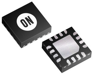
NB6L11SMNG
Fanout Buffer IC, Translator, 2 GHz, CML, LVCMOS, LVDS, LVPECL, LVTTL , 2 Outputs, 2.5 V, QFN-16
- RoHS 10 Compliant
- Tariff Charges
The NB6L11 is an enhanced differential 1:2 clock or data fan-out buffer/translator. The device has the same pin-out and is functionally equivalent to the LVEL11, EP11 and LVEP11 devices. Moreover, the device is optiminzed for the systems that require LOW skew, LOW jitter and LOW power consumtion.Differential input can be configured to accept single-ended signal by applying an external reference voltage to unused complementary input pin. Input accept LVNECL, LVPECL, LVTTL, LVCMOS, CML or LVDS. The outputs are 800mV ECL signals.
- Input Clock Frequency6 GHz
- Input Data Rate 6 Gb/s
- Low 14 mA Typical Power Supply Current
- 150 ps Typical Proagation Delay
- 5 ps Typical Witin Device Skew
- 75 ps Typical Rise/Fall Times
- PECL Mode Operating Range: VCC = 2.375 V to 3.465 V with VEE = 0 V
- NECL Mode Operating Range: VCC = 0 V with VEE = -2.375 V to -3.465 V
- Open Input Default State
- Q Outputs will default LOW with Inputs Open or at VEE
Technical Attributes
Find Similar Parts
| Description | Value | |
|---|---|---|
| Fanout Buffer, Translator | ||
| QFN-EP | ||
| 2 GHz | ||
| CML, LVCMOS, LVDS, LVPECL, LVTTL | ||
| 1 | ||
| 2 | ||
| 16 | ||
| 85 °C | ||
| -40 °C | ||
| LVDS | ||
| NB6L11S Series | ||
| 2.625 Vdc | ||
| 2.375 Vdc |
ECCN / UNSPSC / COO
| Description | Value |
|---|---|
| Country of Origin: | RECOVERY FEE |
| ECCN: | EAR99 |
| HTSN: | 8542390050 |
| Schedule B: | 8542390060 |
