
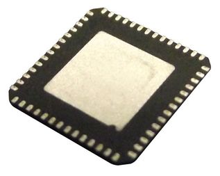
NB3W1900LMNG
Clock Buffer, PCIe Fanout, Zero Delay, 33 MHz to 150 MHz, 19 Outputs, 3.135 V to 3.465 V, 72 Pins, QFN-EP
Click image to enlarge
Manufacturer:onsemi
Product Category:
Clock & Timing, Clock Buffers
Avnet Manufacturer Part #: NB3W1900LMNG
Secondary Manufacturer Part#: NB3W1900LMNG
-
 RoHS 10 Compliant
 -
 Tariff Charges
The NB3W1900L differential clock buffers are designed to work in conjunction with a PCIe compliant source clock synthesizer to provide point-to-point clocks to multiple agents. The device is capable of distributing the reference clocks for Intel® QuickPath Interconnect (Intel QPI), PCIe Gen1/Gen2/Gen3.The NB3W1900L internal PLL is optimized to support 100MHz and 133 MHz frequency operation. The NB3W1900L is developed with the low-power NMOS Push-Pull buffer type.
- 19 Low Power Differential Clock Output Pairs @ 0.7 V
- Output-to-Output Skew Performance: < 85 ps
- Cycle-to-Cycle Jitter (PLL Mode): < 50ps
- Low Phase Jitter (Intel QPI, PCIe Gen 2/Gen 3 Phase Jitter Compliant)
- Input-to-Output Delay Variation: < 50 ps
- Fixed-Feedback for Lowest Input-to-Output Delay Variation
- Spread Spectrum Compatible; Tracks Input Clock Spreading for Low EMI
- 100 MHz and 133 MHz PLL Mode to Meet the Next Generation PCIe Gen2/Gen3 and Intel QPI Phase Jitter
- Individual OE Control via SMBus
- Low-Power NMOS Push-Pull HCSL-Compatible Outputs
- PLL Configurable for PLL Mode or Bypass Mode (Fanout Operation)
- SMBus Address Configurable to Allow Multiple Buffers in a Single Control Network
- Programmable PLL Bandwidth
- Two Tri-level Addresses Selection (Nine SMBus Addresses)
- QFN 72-pin Package, 10 mm × 10 mm
- These are Pb-Free Devices
Technical Attributes
Find Similar Parts
| Description | Value | |
|---|---|---|
| PCIe Fanout Buffer, Zero Delay Buffer | ||
| QFN-EP | ||
| 150 MHz | ||
| 33 MHz | ||
| Differential | ||
| 1 | ||
| 19 | ||
| 72 | ||
| 70 °C | ||
| 0 °C | ||
| HCSL | ||
| NB3W1900L Series | ||
| 3.465 Vdc | ||
| 3.135 Vdc |
ECCN / UNSPSC / COO
| Description | Value |
|---|---|
| Country of Origin: | RECOVERY FEE |
| ECCN: | EAR99 |
| HTSN: | 8542390050 |
| Schedule B: | 8542390060 |