
MC74AC273DTR2G
Octal D Flip-Flop. ONSSPCLGC;
Click image to enlarge
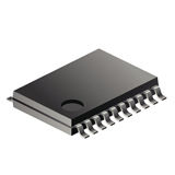
Manufacturer:onsemi
Product Category:
Logic ICs, Flip Flops
Avnet Manufacturer Part #: MC74AC273DTR2G
Secondary Manufacturer Part#: MC74AC273DTR2G
-
 RoHS 10 Compliant
 -
 Tariff Charges

The MC74AC273/74ACT273 has eight edge-triggered D-type flip-flops withindividual D inputs and Q outputs. The common buffered Clock (CP) and MasterReset (MR) inputs load and reset (clear) all flip-flops simultaneously. The register is fully edge-triggered. The state of each D input, one setup timebefore the LOW-to-HIGH clock transition, is transferred to the corresponding flip-flop's Q output. All outputs will be forced LOW independently of Clock or Data inputs by a LOWvoltage level on the MR input. The device is useful for applications where the trueoutput only is required and the Clock and Master Reset are common to all storageelements.
- Ideal Buffer for MOS Microprocessor or Memory
- Eight Edge-Triggered D Flip-Flops
- Buffered Common Clock
- Buffered, Asynchronous Master Reset
- See MC74AC377 for Clock Enable Version
- See MC74AC373 for Transparent Latch Version
- See MC74AC374 for 3-State Version
- Outputs Source/Sink 24 mA
- ACT273 Has TTL Compatible Inputs
- Pb-Free Packages are Available
Technical Attributes
Find Similar Parts
| Description | Value | |
|---|---|---|
| No | ||
| Single-Ended | ||
| Gold | ||
| AC | ||
| D-Type | ||
| 260 °C | ||
| -24 mA | ||
| 10@5V ns | ||
| 8 uA | ||
| 2 V | ||
| Surface Mount | ||
| 1 | ||
| 8 | ||
| 8 | ||
| 8 | ||
| 1 | ||
| 0 | ||
| -40 to 85 to 85 °C | ||
| Single-Ended | ||
| 20WTSSOP | ||
| 20 | ||
| Non-Inverting | ||
| 6.6 x 4.5 x 1.05 mm | ||
| 50 pF | ||
| No | ||
| Industrial | ||
| Master Reset | ||
| WTSSOP | ||
| Positive-Edge | ||
| 5 V |
ECCN / UNSPSC / COO
| Description | Value |
|---|---|
| Country of Origin: | RECOVERY FEE |
| ECCN: | EAR99 |
| HTSN: | 8542390070 |
| Schedule B: | 8542390060 |
 Factory Lead Time: