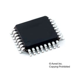
MC10EP195FAG
Delay Line IC, Programmable, 1024 Taps, 10 ps Delay/One Tap, 12.2 ns Total Delay, 3 V to 3.6 V, 32 Pins, LQFP
- RoHS 10 Compliant
- Tariff Charges
NECL/PECL input transition.The delay section consists of a programmable matrix of gates and multiplexers. The delay increment of the EP195 has a digitally selectable resolution of about 10 ps and a range of up to 10.2 ns. The required delay is selected by the 10 data select inputs D(0:9) which are latched on chip by a high signal on the latch enable (LEN) control. The MC10/100EP195 is a programmable delay chip (PDC) designed primarily for clock deskewing and timing adjustment. It provides variable delay of a differential The approximate delay values for varying tap numbers correlating to D0 (LSB) through D9 (MSB). Because the EP195 is designed using a chain of multiplexers it has a fixed minimum delay of 2.2 ns. An additional pin D10 is provided for cascading multiple PDCs for increased programmable range. The cascade logic allows full control of multiple PDCs. Select input pins D0-D10 may be threshold controlled by combinations of interconnects between V (pin 7) and V (pin 8) for CMOS, ECL, or TTL level signals.
- Maximum Frequency > 1.2 Ghz Typical
- Programmable Range: 2.2 ns to 12.2 ns
- 10 ps Increments
- PECL Mode Operating Range: VCC = 3.0 V with VEE = 0 V
- NECL Mode Operating Range: VCC = 0 V with VEE = -3.0 V
- Open Input Default State
- Safety Clamp on Inputs
- A Logic High on the ENbar Pin Will Force Q to Logic Low
- D[0:10] Can Accept Either ECL, CMOS, or TTL Inputs.
- VBB Output Reference Voltage
- Pb-Free Packages are Available
Technical Attributes
Find Similar Parts
| Description | Value |
|---|
ECCN / UNSPSC / COO
| Description | Value |
|---|---|
| Country of Origin: | RECOVERY FEE |
| ECCN: | EAR99 |
| HTSN: | 8542330001 |
| Schedule B: | 8542330000 |
