
FDC6331L
Integrated Load Switch
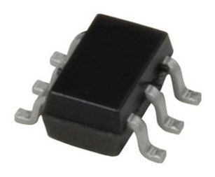
Click image to enlarge
Manufacturer:onsemi
Product Category:
Power Management, Power Load Distribution Switches
Avnet Manufacturer Part #: FDC6331L
Secondary Manufacturer Part#: FDC6331L
-
 RoHS 10 Compliant
 -
 Tariff Charges
The FDC6331L is an Integrated Load Switch for compact power management in portable electronic equipment where 2.5 to 8V input and 2.8A output current capability are needed. This load switch integrates a small N-channel power MOSFET (Q1) that drives a large P-Channel power MOSFET (Q2). This product is general usage and suitable for many different applications.
- Control MOSFET (Q1) includes Zener protection for ESD ruggedness (6kV human body model)
- High performance trench technology for extremely low RDS (ON)
Technical Attributes
Find Similar Parts
| Description | Value | |
|---|---|---|
| 2.8 A | ||
| 2.5 to 8 V | ||
| Matte Tin | ||
| 260 | ||
| 2.8 A | ||
| Surface Mount | ||
| MSL 1 - Unlimited | ||
| 2 | ||
| 2 | ||
| 6 | ||
| 1 | ||
| 100 mOhm | ||
| -55 to 150 °C | ||
| 150 °C | ||
| -55 °C | ||
| 6SuperSOT | ||
| 6 | ||
| 3 x 1.7 x 1 mm | ||
| SuperSOT | ||
| 3.8 Ohm |
ECCN / UNSPSC / COO
| Description | Value |
|---|---|
| Country of Origin: | RECOVERY FEE |
| ECCN: | EAR99 |
| HTSN: | 8541290040 |
| Schedule B: | 8541290080 |