
74LCX112MTC
Low Voltage Dual J-K Negative Edge-Triggered Flip-Flop with 5V Tolerant Inputs
-
 RoHS 10 Compliant
 -
 Tariff Charges
The 74LCX112 is a Low Voltage Dual J-K Negative Edge-Triggered Flip-Flop with 5V Tolerant Inputs The LCX112 is a dual J-K flip-flop. Each flip-flop has independent J, K, PRESET, CLEAR, and CLOCK inputs with Q, Q# outputs. These devices are edge sensitive and change state on the negative going transition of the clock pulse. Clear and preset are independent of the clock and accomplished by a low logic level on the corresponding input. LCX devices are designed for low voltage (3.3V or 2.5) operation with the added capability of interfacing to a 5V signal environment The 74LCX112 is fabricated with advanced CMOS technology to achieve high speed operation while maintaining CMOS low power dissipation.
- 5V tolerant inputs
- 2.3V-3.6V VCC specifications provided
- 7.5 ns tPD max (VCC = 3.3V), 10 µA ICC max
- Power down high impedance inputs and outputs
- ±24 mA output drive (VCC = 3.0V)
- Implements patented noise/EMI reduction circuitry
- Latch-up performance exceeds 500 mA
- ESD performance: Human body model > 2000V Machine model > 2000V
Technical Attributes
Find Similar Parts
| Description | Value | |
|---|---|---|
| No | ||
| Single-Ended | ||
| Gold | ||
| LCX | ||
| JK-Type | ||
| 260 | ||
| -24 mA | ||
| 8@2.7V|7.5@3.3V ns | ||
| 0.01 mA | ||
| Surface Mount | ||
| MSL 1 - Unlimited | ||
| 2 | ||
| 2 | ||
| 1 | ||
| 2 | ||
| 0 | ||
| -40 to 85 °C | ||
| Differential | ||
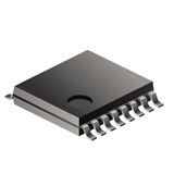
| 16TSSOP | ||
| 16 | ||
| Inverting|Non-Inverting | ||
| 5 x 4.4 x 0.9 mm | ||
| 50 pF | ||
| No | ||
| Set, Reset | ||
| TSSOP | ||
| Negative-Edge | ||
| 2.5|3.3 V |
ECCN / UNSPSC / COO
| Description | Value |
|---|---|
| Country of Origin: | PROJECTED FEE |
| ECCN: | EAR99 |
| HTSN: | 8542390090 |
| Schedule B: | 8542390060 |