
LPC3143FET180,551
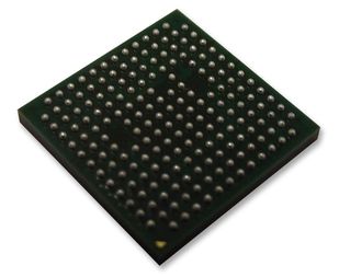
MCU 32-bit LPC3100 ARM926EJ-S RISC ROMLess 1.2V 180-Pin TFBGA Tray
Click image to enlarge
Manufacturer:NXP
Product Category:
Microcontrollers, ARM Microcontrollers
Avnet Manufacturer Part #: LPC3143FET180,551
Secondary Manufacturer Part#: LPC3143FET180,551
-
 RoHS 10 Compliant
 -
 Tariff Charges
The NXP LPC3143 combine a 270 MHz ARM926EJ-S CPU core, High-speed USB 2.0 OTG, 192 KB SRAM, NAND flash controller, flexible external bus interface, four channel 10-bit A/D, and a myriad of serial and parallel interfaces in a single chip targeted at consumer, industrial, medical, and communication markets. To optimize system power consumption, the LPC3143 have multiple power domains and a very flexible Clock
- 270 MHz, 32-bit ARM926EJ-S
- 16 kB D-cache and 16 kB I-cache
- Memory Management Unit (MMU)
- 192 kB embedded SRAM
- NAND flash controller with 8-bit ECC and AES decryption support
- AES decryption engine
- Secure one-time programmable memory for AES key storage and customer use
- 128 bit unique ID per device for DRM schemes
- 8/16-bit Multi-Port Memory Controller (MPMC): SDRAM and SRAM
- High-speed USB 2.0 (OTG, Host, Device) with on-chip PHY
- Two I2S interfaces
- Integrated master/slave SPI
- Two master/slave I2C-bus interfaces
- Fast UART
- Memory Card Interface (MCI): MMC/SD/SDIO/CE-ATA
- Four-channel 10-bit ADC
- Integrated 4/8/16-bit 6800/8080 compatible LCD interface
- Dynamic clock gating and scaling
- Multiple power domains
- Selectable boot-up: SPI flash, NAND flash, SD/MMC cards, UART, or USB
- Secure booting using an AES decryption engine
Technical Attributes
Find Similar Parts
| Description | Value | |
|---|---|---|
| 32 Bit | ||
| ARM926EJ-S | ||
| TFBGA | ||
| Surface Mount | ||
| I2C/I2S/SPI/UART/USB | ||
| LPC | ||
| LPC3000 | ||
| 180 | ||
| 270 | ||
| 85 °C | ||
| -40 °C | ||
| LPC Family LPC3000 Series Microcontrollers |
ECCN / UNSPSC / COO
| Description | Value |
|---|---|
| Country of Origin: | RECOVERY FEE |
| ECCN: | 3A991.A.2 |
| HTSN: | 8542310025 |
| Schedule B: | 8542310025 |