
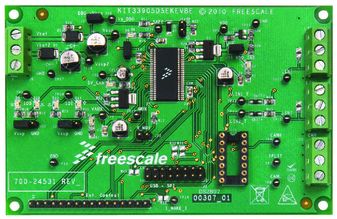
KIT33905D5EKEVBE
System Basis Chip Gen2
Click image to enlarge
Manufacturer:NXP
Product Category:
Kits & Tools, Evaluation & Development Kits
Avnet Manufacturer Part #: KIT33905D5EKEVBE
Secondary Manufacturer Part#: KIT33905D5EKEVBE
-
 RoHS 10 Compliant
 -
 Tariff Charges
The KIT33905D5EKEVBE supports the 33905D5 and 33904 devices, which are the second generation family of System Basis Chips, which combine several features and enhance present module designs. The devices work as an advanced power management unit for the MCU and additional integrated circuits such as sensors, CAN transceivers. They have a built-in enhanced high speed CAN interface (ISO11898-2 and -5), with local and bus failure diagnostics, protection, and fail safe operation mode. The SBCs may include one or two LIN 2.0 interfaces with LIN output pin switches. The 33904/5 include 2 or 3 wake-up input pins than can also be configured as output drivers for flexibility.
- Nominal operating supply voltage range of 5.5 V to 27 V
- Individually routed power supply inputs for VSUP1 and VSUP2
- 5.0/3.3 V regulator for MCU with an external PNP ballast transistor to increase current capability
- Multiple CAN Bus termination options supported via socket
- Two high/low side I/Os (SPI configurable) accessible through test points
- Status of I/O-0 and I/O-1 indicated by an LED (dependent on jumper configuration)
- Debug mode/watchdog configuration via jumper settings
- MUX output voltage accessible through a test point and external resistor selectable through jumper
- 3.3 V or 5.0 V output voltage test point VAUX (SPI configurable)
- I_WAKE_I test point to enable a FET and load VDD with current to wake-up the SBC
- LIN1_T and LIN2_T test points to monitor I/O voltages (SPI configurable)
- I/O-0, I/O-1, VAUX, 5V_CAN, SAFE, and VDD status indicated by LED
- 100 mil 2x8 pin standard heade
Technical Attributes
Find Similar Parts
| Description | Value | |
|---|---|---|
| System Basis Chip Gen2 | ||
| System Basis Chip Gen2 |
ECCN / UNSPSC / COO
| Description | Value |
|---|---|
| Country of Origin: | NO RECOVERY FEE |
| ECCN: | EAR99 |
| HTSN: | 8473301180 |
| Schedule B: | 8473300002 |