
NXB0102DC-Q100H
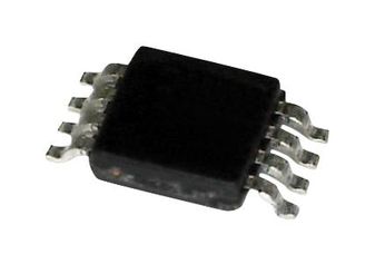
Translating Transceiver, 2 Inputs, 1.65 V to 5.5 V Supply, VSSOP-8, -40 °C to 125 °C
-
 RoHS 10 Compliant
 -
 Tariff Charges
NXB0102DC-Q100H is a 2bit, dual supply translating transceiver with auto direction sensing, that enables bidirectional voltage level translation. It features two 2bit input-output ports (An and Bn), one output enable input (OE) and two supply pins (VCC(A) and VCC(B)). VCC(A) can be supplied at any voltage between 1.2V and 3.6V and VCC(B) can be supplied at any voltage between 1.65V and 5.5V, making the device suitable for translating between any of the low voltage nodes (1.2V, 1.5V, 1.8V, 2.5V, 3.3V and 5V). Pins An and OE are referenced to VCC(A) and pins Bn are referenced to VCC(B). A LOW level at pin OE causes the outputs to assume a high-impedance OFF-state. This device is fully specified for partial power-down applications using IOFF. This product has been qualified to the automotive electronics council (AEC) standard Q100 (Grade 1) and is suitable for use in automotive applications.
- Wide supply voltage range: VCC(A): 1.2V to 3.6V and VCC(B): 1.65V to 5.5V
- IOFF circuitry provides partial power-down mode operation
- Inputs accept voltages upto 5.5V, ESD protection
- Latch-up performance exceeds 100mA per JESD 78B Class II
- Input leakage current is ±1µA max at (OE input;VI = 0V to 3.6V;VCC(A) = 1.2V to 3.6V)
- Input capacitance is 2pF typ at (OE input;VCC(A) = 1.2V to 3.6V;VCC(B) = 1.65V to 5.5V)
- Supply current is 3µA max at (VCC(A) = 1.4V to 3.6V;VCC(B) = 1.65V to 5.5V, -40°C to +85°C)
- Propagation delay is 7.5ns (A to B, 1.8V, VCC(A) = 1.2V; Tamb = 25°C)
- Operating temperature range from -40°C to +125°C
- VSSOP8 package
Technical Attributes
Find Similar Parts
| Description | Value |
|---|
ECCN / UNSPSC / COO
| Description | Value |
|---|---|
| Country of Origin: | RECOVERY FEE |
| ECCN: | EAR99 |
| HTSN: | 8542390050 |
| Schedule B: | 8542390060 |