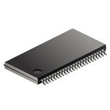
74LVC16373ADGG-Q1J
Latch, 74LVC16373, D Type Transparent, Tri State Non Inverted, 5.5 ns, 24 mA, 48 Pins, TSSOP
The 74LVC16373A-Q100 and 74LVCH16373A-Q100 are 16-bit D-type transparent latches featuring separate D-type inputs with bus hold (74LVCH16373A-Q100 only) for each latch and 3-state outputs for bus-oriented applications. One Latch Enable (LE) input and one Output Enable are provided for each octal. Inputs can be driven from either 3.3 V or 5 V devices. When disabled, up to 5.5 V can be applied to the outputs. These features allow the use of these devices in mixed 3.3 V and 5 V applications. The device consists of two sections of eight D-type transparent latches with 3-state true outputs. When LE is HIGH, data at the Dn inputs enter the latches. In this condition, the latches are transparent, that is, the latch outputs change each time its corresponding D-input changes. The latches store the information that was present at the D-inputs one set-up time (tsu) preceding the HIGH-to-LOW transition of LE. When Output Enable is LOW, the contents of the eight latches are available at the outputs. When Output Enable is HIGH, the outputs go to the high impedance OFF-state. Operation of the Output Enable input does not affect the state of the latches. Bus hold on the data inputs eliminates the need for external pull-up resistors to hold unused inputs. This product has been qualified to the Automotive Electronics Council (AEC) standard Q100 (Grade 1) and is suitable for use in automotive applications.
- Automotive product qualification in accordance with AEC-Q100 (Grade 1)
- Specified from -40 °C to +85 °C and from -40 °C to +125 °C
- 5 V tolerant inputs/outputs for interfacing with 5 V logic
- Wide supply voltage range from 1.2 V to 3.6 V
- CMOS low power consumption
- Multibyte flow-through standard pinout architecture
- Multiple low inductance supply pins for minimum noise and ground bounce
- Direct interface with TTL levels
- All data inputs have bus hold (74LVCH16373A-Q100 only)
- High-impedance when VCC =0V
- Complies with JEDEC standard:
- JESD8-7A (1.65 V to 1.95 V)
- JESD8-5A (2.3 V to 2.7 V)
- JESD8-C/JESD36 (2.7 V to 3.6 V)
Technical Attributes
Find Similar Parts
| Description | Value | |
|---|---|---|
| No | ||
| Transparent | ||
| Gold over Nickel Palladium | ||
| LVC | ||
| 260 | ||
| -24 mA | ||
| 24 mA | ||
| 2.9(Typ)@2.7V|2.4(Typ)@3.3V ns | ||
| Surface Mount | ||
| MSL 1 - Unlimited | ||
| 16 | ||
| 2 | ||
| 1 | ||
| 16 | ||
| 1 | ||
| 16 | ||
| 0 | ||
| -40 to 125 °C | ||
| 3-State | ||
| 48TSSOP | ||
| 48 | ||
| Non-Inverting | ||
| 12.6(Max) x 6.2(Max) x 1.05(Max) | ||
| 50 pF | ||
| No | ||
| TSSOP | ||
| 5 V | ||
| D-Type |
ECCN / UNSPSC / COO
| Description | Value |
|---|---|
| Country of Origin: | RECOVERY FEE |
| ECCN: | EAR99 |
| HTSN: | 8542390050 |
| Schedule B: | 8542390060 |
