
74HCT273PW-Q100J
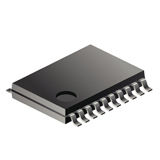
Flip Flop, 74HCT273, D, 15 ns, 56 MHz, 5.2 mA, 20 Pins, TSSOP
-
 RoHS 10 Compliant
 -
 Tariff Charges

The 74HC273-Q100; 74HCT273-Q100 is an octal positive-edge triggered D-type flip-flop. The device features clock (CP) and master reset (MR) inputs. The outputs Qn assume the state of their corresponding Dn inputs that meet the set-up and hold time requirements on the LOW-to-HIGH clock (CP) transition. A LOW on MR forces the outputs LOW independently of clock and data inputs. Inputs include clamp diodes which enable the use of current limiting resistors to interface inputs to voltages in excess of VCC. This product has been qualified to the Automotive Electronics Council (AEC) standard Q100 (Grade 1) and is suitable for use in automotive applications.
- Automotive product qualification in accordance with AEC-Q100 (Grade 1)
- Specified from -40 °C to +85 °C and from -40 °C to +125 °C
- Input levels:
- For 74HC273-Q100: CMOS level
- For 74HCT273-Q100: TTL level
- Common clock and master reset
- Eight positive edge-triggered D-type flip-flops
- Complies with JEDEC standard no. 7A
- ESD protection:
- HBM JESD22-A114F exceeds 2000 V
- MM JESD22-A115-A exceeds 200 V
- Multiple package options
Technical Attributes
Find Similar Parts
| Description | Value | |
|---|---|---|
| No | ||
| Single-Ended | ||
| Gold over Nickel Palladium | ||
| HCT | ||
| D-Type Bus Interface | ||
| 260 | ||
| -4 mA | ||
| 30@4.5V ns | ||
| 0.008 mA | ||
| Surface Mount | ||
| MSL 1 - Unlimited | ||
| 8 | ||
| 8 | ||
| 8 | ||
| 1 | ||
| 0 | ||
| -40 to 125 °C | ||
| Single-Ended | ||
| 20TSSOP | ||
| 20 | ||
| Non-Inverting | ||
| 6.6(Max) x 4.5(Max) x 0.95(Max) | ||
| 50 pF | ||
| No | ||
| Automotive | ||
| Master Reset | ||
| TSSOP | ||
| Positive-Edge | ||
| 5 V |
ECCN / UNSPSC / COO
| Description | Value |
|---|---|
| Country of Origin: | RECOVERY FEE |
| ECCN: | EAR99 |
| HTSN: | 8542390050 |
| Schedule B: | 8542390060 |
 Factory Lead Time: