
74HC73PW,118
Flip Flop, 74HC73, JK, 27 ns, 83 MHz, 5.2 mA, 14 Pins, TSSOP
-
 RoHS 10 Compliant
 -
 Tariff Charges
The 74HC73 is a high-speed Si-gate CMOS device that complies with JEDEC standard no. 7A. It is pin compatible with Low-power Schottky TTL (LSTTL). The 74HC73 is a dual negative-edge triggered JK flip-flop featuring individual J, K, clock (nCP) and reset (nR) inputs; also complementary nQ and nQ outputs. The J and K inputs must be stable one set-up time prior to the HIGH-to-LOW clock transition for predictable operation. The reset (nR) is an asynchronous active LOW input. When LOW, it overrides the clock and data inputs, forcing the nQ output LOW and the nQ output HIGH. Schmitt-trigger action in the clock input makes the circuit highly tolerant to slower clock rise and fall times.
- Low-power dissipation
- Complies with JEDEC standard no. 7A
- ESD protection:
- HBM JESD22-A114E exceeds 2000 V
- MM JESD22-A115-A exceeds 200 V
- Multiple package options
- Specified from -40 °C to +80 °C and from -40 °C to +125 °C
Technical Attributes
Find Similar Parts
| Description | Value | |
|---|---|---|
| No | ||
| Single-Ended | ||
| Gold | ||
| HC | ||
| JK-Type | ||
| 260 | ||
| -5.2 mA | ||
| 160@2V|32@4.5V|27@6V ns | ||
| 0.004 mA | ||
| Surface Mount | ||
| MSL 1 - Unlimited | ||
| 2 | ||
| 2 | ||
| 1 | ||
| 2 | ||
| 0 | ||
| -40 to 125 °C | ||
| Differential | ||
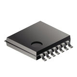
| 14TSSOP | ||
| 14 | ||
| Inverting|Non-Inverting | ||
| 5.1 x 4.5 x 0.95 mm | ||
| 50 pF | ||
| No | ||
| Reset | ||
| TSSOP | ||
| Negative-Edge | ||
| 5 V |
ECCN / UNSPSC / COO
| Description | Value |
|---|---|
| Country of Origin: | RECOVERY FEE |
| ECCN: | EAR99 |
| HTSN: | 8542390050 |
| Schedule B: | 8542390060 |