
74HC4094D,653
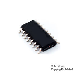
Shift Register, 74HC4094, Serial to Parallel, Serial to Serial, 1 Element, 8 -Bit, 16 Pins, SOIC
-
 RoHS 10 Compliant
 -
 Tariff Charges
The 74HC4094D is an 8 stage shift and store bus register in 16 pin SOIC package. It is a 8bit serial in/serial or parallel out shift register with a storage register and 3 state outputs. Both shift and storage register have separate clocks. The device features a serial input (D) and two serial outputs (QS1 and QS2) to enable cascading. Data is shifted on low to high transitions of CP input. Data is available at QS1 on LOW to HIGH transitions of CP input to allow cascading when clock edges are fast. The same data is available at QS2 on next HIGH to LOW transition of CP input to allow cascading when clock edges are slow. The data in the shift register is transferred to storage register when STR input is high. Data in storage register appears at outputs whenever the output enable input (OE) is high. A low on OE causes the outputs to assume high impedance OFF state. Typical application includes serial to parallel data conversion and remote control holding register.
- Low-power dissipation
- CMOS Input level
- Complies with JEDEC standard No. 7A
Technical Attributes
Find Similar Parts
| Description | Value | |
|---|---|---|
| Uni-Directional | ||
| Gold | ||
| HC | ||
| Latch/Shift Register | ||
| 260 °C | ||
| 26@6V ns | ||
| 8 uA | ||
| Surface Mount | ||
| MSL 1 - Unlimited | ||
| 0 | ||
| 1 | ||
| 10 | ||
| 1 | ||
| 0 | ||
| 8 | ||
| 2 to 6 V | ||
| -40 to 125 °C | ||
| Serial to Serial/Parallel | ||
| 3-State | ||
| 16SO | ||
| No | ||
| 16 | ||
| 10 x 4 x 1.45 mm mm | ||
| 50 pF | ||
| No | ||
| Extended Industrial | ||
| SOIC | ||
| No | ||
| Positive-Edge | ||
| Octal | ||
| 5 V |
ECCN / UNSPSC / COO
| Description | Value |
|---|---|
| Country of Origin: | RECOVERY FEE |
| ECCN: | EAR99 |
| HTSN: | 8542390050 |
| Schedule B: | 8542390060 |