
74HC4053PW-Q100,11
Analog Multiplexer Triple 2:1 16-Pin TSSOP T/R
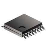
-
 RoHS 10 Compliant
 -
 Tariff Charges

The 74HC4053-Q100; 74HCT4053-Q100 is a high-speed Si-gate CMOS device and is pin compatible with Low-power Schottky TTL (LSTTL). It is specified in compliance with JEDEC standard no. 7A. The 74HC4053-Q100; 74HCT4053-Q100 is triple 2-channel analog multiplexer/demultiplexer with a common enable input. Each multiplexer/demultiplexer has two independent inputs/outputs (nY0 and nY1), a common input/output (nZ) and three digital select inputs (Sn). With enable input LOW, one of the two switches is selected (low-impedance ON-state) by S1 to S3. With enable input HIGH, all switches are in the high-impedance OFF-state, independent of S1 to S3. VCC and GND are the supply voltage pins for the digital control inputs. The VCC to GND ranges are 2.0 V to 10.0 V for 74HC4053-Q100, and 4.5 V to 5.5 V for 74HCT4053-Q100. The analog inputs/outputs (nY0 to nY1, and nZ) can swing between VCC as a positive limit and VEE as a negative limit. VCC - VEE may not exceed 10.0 V. For operation as a digital multiplexer/demultiplexer, VEE is connected to GND (typically ground). This product has been qualified to the Automotive Electronics Council (AEC) standard Q100 (Grade 1) and is suitable for use in automotive applications.
- Automotive product qualification in accordance with AEC-Q100 (Grade 1)
- Specified from -40 °C to +85 °C and from -40 °C to +125 °C
- Wide analog input voltage range from -5 V to +5 V
- Low ON resistance:
- 80 ? (typical) at VCC - VEE = 4.5 V
- 70 ? (typical) at VCC - VEE = 6.0 V
- 60 ? (typical) at VCC - VEE = 9.0 V
- Logic level translation: to enable 5 V logic to communicate with ± 5 V analog signals
- Typical ‘break before make’ built-in
- ESD protection:
- MIL-STD-883, method 3015 exceeds 2000 V
- HBM JESD22-A114F exceeds 2000 V
- MM JESD22-A115-A exceeds 200 V (C = 200 pF, R = 0 ?)
- CDM AEC-Q100-011 revision B exceeds 1000 V
- Multiple package options
Technical Attributes
Find Similar Parts
| Description | Value | |
|---|---|---|
| Triple 2:1 | ||
| Gold | ||
| 260 | ||
| 180@4.5V Ohm | ||
| 220@2V ns | ||
| Surface Mount | ||
| MSL 1 - Unlimited | ||
| 6 | ||
| 3 | ||
| 0.016@10V mA | ||
| ±5|10|±1|2|±2.5|5 V | ||
| -40 to 125 °C | ||
| 16TSSOP | ||
| 16 | ||
| Single|Dual | ||
| 5.1 x 4.5 x 0.95 mm | ||
| No | ||
| TSSOP | ||
| 2V to 10V, ± 5V |
ECCN / UNSPSC / COO
| Description | Value |
|---|---|
| Country of Origin: | RECOVERY FEE |
| ECCN: | EAR99 |
| HTSN: | 8542390050 |
| Schedule B: | 8542390060 |
 Factory Lead Time: