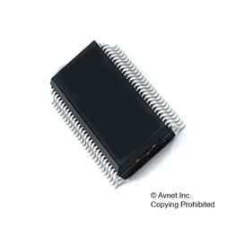
74ALVT162821DL,518
Flip Flop, 74ALVT162821, D, 5 ns, 150 MHz, 12 mA, 56 Pins, SSOP
- RoHS 10 Compliant
- Tariff Charges
The 74ALVT162821 high-performance BiCMOS device combines low static and dynamic power dissipation with high speed and high output drive. It is designed for VCC operation at 2.5V or 3.3V with I/O compatibility to 5V. The 74ALVT162821 has two 10-bit, edge triggered registers, with each register coupled to a 3-State output buffer. The two sections of each register are controlled independently by the clock (nCP) and Output Enable (nOE) control gates. Each register is fully edge triggered. The state of each D input, one set-up time before the Low-to-High clock transition, is transferred to the corresponding flip-flop's Q output. The 3-State output buffers are designed to drive heavily loaded 3-State buses, MOS memories, or MOS microprocessors. The active Low Output Enable (nOE) controls all ten 3-State buffers independent of the register operation. When nOE is Low, the data in the register appears at the outputs. When nOE is Highthe outputs are in high impedance "off"" state, which means they will neither drive nor load the bus. The 74ALVT162821 is designed with 30 O series resistance in both High and Low output stages. This design reduces the line noise in applications such as memory address drivers, clock drivers and bus receivers/transmitters. The series termination resistors reduce overshoot and undershoot and are ideal for driving memory arrays."
- Outputs include series resistance of 30 O making external termination resistors unnecessary
- 20-bit positive-edge triggered register
- 5 V I/O Compatible
- Multiple VCC and GND pins minimize switching noise
- Live insertion/extraction permitted
- Power-up reset
- Power-up 3-State
- Output capability ±12 mA
- Latch-up protection exceeds 500 mA per Jedec Std 17
- ESD protection exceeds 2000 V per MIL STD 883 Method 3015 and 200 V per Machine Model
- Bus hold data inputs eliminate the need for external pull-up resistors to hold unused inputs
Technical Attributes
Find Similar Parts
| Description | Value |
|---|
ECCN / UNSPSC / COO
| Description | Value |
|---|---|
| Country of Origin: | RECOVERY FEE |
| ECCN: | EAR99 |
| HTSN: | 8542330001 |
| Schedule B: | 8542330000 |
