
74ALVCH16601DGG:11
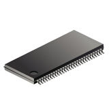
Transceiver, Non Inverting, 74ALVCH16601, 1 Element, 2.3 V to 3.6 V, 56 Pins, TSSOP
-
 RoHS 10 Compliant
 -
 Tariff Charges
The 74ALVCH16601 is an 18-bit universal transceiver featuring non-inverting 3-State bus compatible outputs in both send and receive directions. Data flow in each direction is controlled by output enable (OEAB and OEBA), latch enable (LEAB and LEBA), and clock (CPAB and CPBA) inputs. For A-to-B data flow, the device operates in the transparent mode when LEAB is High. When LEAB is Low, the A data is latched if CPAB is held at a High or Low logic level. If LEAB is Low, the A-bus data is stored in the latch/flip-flop on the Low-to-High transition of CPAB. When OEAB is Low, the outputs are active. When OEAB is High, the outputs are in the high-impedance state. The clocks can be controlled with the clock-enable inputs (CEBA/CEAB). Data flow for B-to-A is similar to that of A-to-B but uses OEBA, LEBA and CPBA. To ensure the high impedance state during power up or power down, OEBA and OEAB should be tied to VCC through a pullup resistor; the minimum value of the resistor is determined by the current-sinking/current-sourcing capability of the driver. Active bus-hold circuitry is provided to hold unused or floating data inputs at a valid logic level.
- Complies with JEDEC standard no. 8-1A
- CMOS low power consumption
- Direct interface with TTL levels
- MULTIBYTETM flow-through standard pin-out architecture
- Low inductance multiple VCC and ground pins for minimum noise and ground bounce
- Current drive ± 24 mA at 3.0 V
- All inputs have bus hold circuitry
- Output drive capability 50? transmission lines @ 85°C
Technical Attributes
Find Similar Parts
| Description | Value | |
|---|---|---|
| TSSOP | ||
| Transceiver, Non Inverting | ||
| 74ALVCH16601 | ||
| 7416601 | ||
| 74ALVCH | ||
| 1 Element | ||
| 18bit | ||
| 56 | ||
| 85 °C | ||
| -40 °C | ||
| 3.6 V | ||
| 2.3 V |
ECCN / UNSPSC / COO
| Description | Value |
|---|---|
| Country of Origin: | RECOVERY FEE |
| ECCN: | EAR99 |
| HTSN: | 8542390050 |
| Schedule B: | 8542390060 |