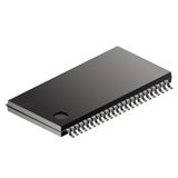
NAND02GW3B2DN6E
Flash Mem Parallel 3V 2G-Bit 256M x 8 25us 48-Pin TSOP Tray
- RoHS 10 Compliant
- Tariff Charges
The NAND02G-B2D devices are part of the NAND flash 2112-byte/1056-word page family of non-volatile flash memories. They use NAND cell technology and have a density of 2 Gbits. These devices have a memory array that is split into 2 planes of 1024 blocks each. This multiplane architecture makes it possible to program 2 pages at a time (one in each plane), or to erase 2 blocks at a time (one in each plane). This feature reduces the average program and erase times by 50%. The NAND02G-B2D devices operate from a 1.8 V or 3 V voltage supply. Depending on whether the device has a x8 or x16 bus width, the page size is 2112 bytes (2048 + 64 spare) or 1056 words (1024 + 32 spare), respectively. The address lines are multiplexed with the data input/output signals on a multiplexed x 8 input/output bus. This interface reduces the pin count and makes it possible to migrate to other densities without changing the footprint. Each block can be programmed and erased over 100,000 cycles with ECC (error correction code) on. To extend the lifetime of NAND flash devices, the implementation of an ECC is mandatory. A write protect pin is available to provide hardware protection against program and erase operations. The devices feature an open-drain ready/busy output that identifies if the P/E/R (program/erase/read) controller is currently active. The use of an open-drain output allows the ready/busy pins from several memories to connect to a single pull-up resistor. A Copy Back Program command is available to optimize the management of defective blocks. When a page program operation fails, the data can be programmed in another page without having to resend the data to be programmed. An embedded error detection code is automatically executed after each copy back operation: 1 error bit can be detected for every 528 bits. With this feature it is no longer necessary to use an external 2-bit ECC to detect copy back operation errors. The devices have a cache read feature that i
- High density NAND flash memory
- Up to 2 Gbits of memory array
- Cost-effective solution for mass storage applications
- NAND interface
- x8 or x16 bus width
- Multiplexed address/data
- Supply voltage: 1.8 V or 3.0 V device
- Page size
- x8 device: (2048 + 64 spare) bytes
- x16 device: (1024 + 32 spare) words
- Block size
- x8 device: (128 K + 4 K spare) bytes
- x16 device: (64 K + 2 K spare) words
- Multiplane architecture
- Array split into two independent planes
- Program/erase operations can be performed on both planes at the same time
- Page read/program
- Random access: 25 µs (max)
- Sequential access: 25 ns (min)
- Page program time: 200 µs (typ)
- Multiplane page program time (2 pages) 200 µs (typ)
- Copy back program with automatic EDC (error detection code)
- Cache read mode<
Technical Attributes
Find Similar Parts
| Description | Value |
|---|
ECCN / UNSPSC / COO
| Description | Value |
|---|---|
| Country of Origin: | null |
| ECCN: | 3A991 |
| HTSN: | 8542320071 |
| Schedule B: | 8542320050 |
