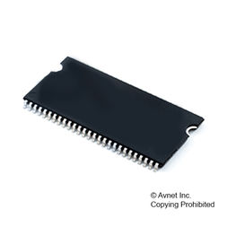
MT48LC4M16A2P-6A:J
DRAM, SDR, 64 Mbit, 4M x 16bit, 167 MHz, 54 Pins, TSOP-II
MT48LC4M16A2P-6A:J is a SDR SDRAM. The 64Mb SDRAM is a high-speed CMOS, dynamic random-access memory containing 67,108,864 bits. It is internally configured as a quad-bank DRAM with a synchronous interface (all signals are registered on the positive edge of the clock signal, CLK). Each of the x4’s 16,777,216-bit banks are organized as 4096 rows by 1024 columns by 4 bits. Each of the x8’s 16,777,216-bit banks are organized as 4096 rows by 512 columns by 8 bits. Each of the x16’s 16,777,216-bit banks are organized as 4096 rows by 256 columns by 16 bits. The 64Mb SDRAM is designed to operate in 3.3V memory systems. An auto refresh mode is provided, along with a power-saving, power-down mode. All inputs and outputs are LVTTL-compatible.
- Fully synchronous; all signals registered on positive edge of system clock
- Internal, pipelined operation; column address can be changed every clock cycle
- Internal banks for hiding row access/precharge
- Auto precharge, includes concurrent auto precharge and auto refresh modes
- LVTTL-compatible inputs and outputs
- Single 3.3V ±0.3V power supply
- Timing – cycle time : 6ns at CL = 3
- 4 Meg x 16
- 54-pin TSOP II package
- Commercial operating temperature range from 0°C to +70°C
Technical Attributes
Find Similar Parts
| Description | Value | |
|---|---|---|
| 14 Bit | ||
| 16 Bit | ||
| 64 Mbit | ||
| Tin | ||
| 260 | ||
| 167 MHz | ||
| 5.4 ns | ||
| Surface Mount | ||
| 16 Bit | ||
| 16 Bit | ||
| 3.3 V | ||
| 0 to 70 °C | ||
| 54TSOP-II | ||
| 54 | ||
| 22.22 x 10.16 x 1 mm | ||
| Commercial | ||
| TSOP-II | ||
| SDRAM |
ECCN / UNSPSC / COO
| Description | Value |
|---|---|
| Country of Origin: | PROJECTED FEE |
| ECCN: | EAR99 |
| HTSN: | 8542320002 |
| Schedule B: | 8542320015 |
