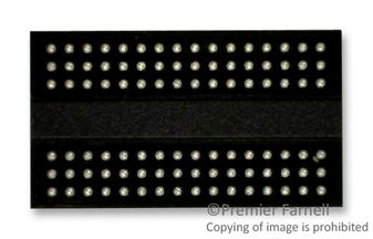
MT47H32M16NF-25E IT:H
DRAM, DDR2, 512 Mbit, 32M x 16bit, 400 MHz, TFBGA, 84 Pins
MT47H32M16NF-25E IT:H is a DDR2 SDRAM. It uses a double data rate architecture to achieve high-speed operation. The double data rate architecture is essentially for 4n-prefetch architecture, with an interface designed to transfer two data words per clock cycle at the I/O balls. A single READ or WRITE operation for the DDR2 SDRAM consists of a single 4n-bitwide, two-clock-cycle data transfer at the internal DRAM core and four corresponding n-bit-wide, one-half-clock-cycle data transfers at the I/O balls. It has JEDEC-standard 1.8V I/O (SSTL_18-compatible) with differential data strobe (DQS, DQS#) option.
- Operating voltage range is 1.8V (VDD)
- 32Meg x 16 configuration, adjustable data-output drive strength
- Packaging style is 84-ball 8mm x 12.5mm FBGA
- Timing (cycle time) is 2.5ns at CL = 5 (DDR2-800)
- 4n-bit prefetch architecture
- Data rate is 800MT/s
- DLL to align DQ and DQS transitions with CK, programmable CAS latency (CL)
- Posted CAS additive latency (AL), WRITE latency = READ latency - 1?CK
- Adjustable data-output drive strength, 64ms, 8192-cycle refresh
- On-die termination (ODT), supports JEDEC clock jitter specification
Technical Attributes
Find Similar Parts
| Description | Value | |
|---|---|---|
| 13 Bit | ||
| 400 MHz | ||
| 16 Bit | ||
| 512 Mbit | ||
| DDR2 SDRAM | ||
| FBGA | ||
| Surface Mount | ||
| Tin-Silver-Copper | ||
| 260 | ||
| 400 MHz | ||
| 0.4 ns | ||
| 32M x 16bit | ||
| 512 Mbit | ||
| Surface Mount | ||
| 84 | ||
| 16 Bit | ||
| 16 Bit | ||
| 1.8 V | ||
| -40 to 85 °C | ||
| 85 °C | ||
| -40 °C | ||
| 32M x 16 | ||
| 84FBGA | ||
| 84 | ||
| 8 x 12.5 x 0.975 | ||
| Industrial | ||
| FBGA | ||
| 1.8 V | ||
| DDR2 SDRAM |
ECCN / UNSPSC / COO
| Description | Value |
|---|---|
| Country of Origin: | RECOVERY FEE |
| ECCN: | EAR99 |
| HTSN: | 8542320002 |
| Schedule B: | 8542320060 |
