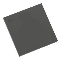
MT29F4G08ABBDAHC-IT:D
Flash Memory, SLC NAND, 4 Gbit, 512M x 8bit, Parallel, VFBGA, 63 Pins
- RoHS 10 Compliant
- Tariff Charges
MT29F4G08 is a NAND flash memory. NAND flash device include an asynchronous data interface for high-performance I/O operations. This device use a highly multiplexed 8-bit bus (I/Ox) to transfer commands, address, and data. There are five control signals used to implement the asynchronous data interface: CE#, CLE, ALE, WE#, and RE#. Additional signals control hardware write protection and monitor device status (R/B#). This hardware interface creates a low pin-count device with a standard pinout that remains the same from one density to another, enabling future upgrades to higher densities with no board redesign. A target is the unit of memory accessed by a chip enable signal. A target contains one or more NAND Flash die. A NAND flash die is the minimum unit that can independently execute commands and report status. A NAND flash die, in the ONFI specification, is referred to as a logical unit (LUN). There is at least one NAND Flash die per chip enable signal.
- Single-level cell (SLC) technology, asynchronous I/O performance
- Array performance, read page is 45µs (typical)
- Command set is ONFI NAND flash protocol, read unique ID
- Operation status byte provides software method for detecting, operation completion
- First block (block address 00h) is valid when shipped from factory
- RESET (FFh) required as first command after power-on, quality and reliability
- Internal data move operations supported within the plane from which data is read
- 4Gb density, 8bit device width, SLC level
- 1.8V (1.7–1.95V) operating voltage, asynchronous interface
- 63-ball VFBGA (10.5 x 13 x 1.0mm) package, industrial operating temperature range from –40° to 85°C
Technical Attributes
Find Similar Parts
| Description | Value | |
|---|---|---|
| 45 ns | ||
| 1 Bit | ||
| Sectored | ||
| Symmetrical | ||
| No | ||
| SLC NAND | ||
| 4 Gbit | ||
| Yes | ||
| No | ||
| SLC NAND | ||
| VFBGA | ||
| Surface Mount | ||
| Parallel | ||
| Parallel | ||
| Tin-Silver-Copper | ||
| 260 | ||
| 0.003/Block s | ||
| 20 mA | ||
| 0.6/Page ms | ||
| 25 ns | ||
| 512M x 8bit | ||
| 4 Gbit | ||
| Surface Mount | ||
| 63 | ||
| 8 Bit | ||
| 512 MWords | ||
| -40 to 85 °C | ||
| 85 °C | ||
| -40 °C | ||
| 63VFBGA | ||
| 63 | ||
| 10.5 x 13 x 0.65 mm | ||
| 1.8V SLC NAND Flash Memories | ||
| 20 mA | ||
| No | ||
| Industrial | ||
| No | ||
| VFBGA | ||
| 1.95 V | ||
| 1.7 V | ||
| 1.8 V | ||
| 1.8000 V |
ECCN / UNSPSC / COO
| Description | Value |
|---|---|
| Country of Origin: | RECOVERY FEE |
| ECCN: | 3A991.B.1.A |
| HTSN: | 8542320051 |
| Schedule B: | 8542320060 |
