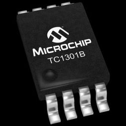
TC1301B-APAVUA
LDO Regulator Pos 3.3V1.8V 0.3A/0.15A 8-Pin MSOP Tube
- RoHS 10 Compliant
- Tariff Charges
The TC1301 combines two Low Dropout (LDO) regulators and a microcontroller RESET function into a single 8-pin MSOP or DFN package. Both regulator outputs feature low dropout voltage, 104 mV @ 300 mA for VOUT1, 150 mV @ 150 mA for VOUT2, low quiescent current consumption, 58 µA each and a typical regulation accuracy of 0.5%. Several fixedoutput voltage and detector voltage combinations are available. A reference bypass pin is available to further reduce output noise and improve the power supply rejection ratio of both LDOs. The TC1301 is stable over all line and load conditions with a minimum of 1 µF of ceramic output capacitance, and utilizes a unique compensation scheme to provide fast dynamic response to sudden line voltage and load current changes. For the TC1301A, the microcontroller RESET function operates independently of both VOUT1 and VOUT2. The input to the RESET function is connected to the VDET pin.The SHDN2 pin is used to control the output of VOUT2 only. VOUT1 will power-up and down with VIN. In the case of the TC1301B, the detect voltage input of the RESET function is connected internally to VOUT1. Both VOUT1 and VOUT2 have independent shutdown capability. Additional features include an overcurrent limit and overtemperature protection that, when combined, provide a robust design for all load fault conditions.
- Dual Output LDO with Microcontroller Reset Monitor Functionality:
- VOUT1 = 1.5V to 3.3V @ 300 mA
- VOUT2 = 1.5V to 3.3V @ 150 mA
- VRESET = 2.20V to 3.20V
- Output Voltage and RESET Threshold Voltage Options Available
- Low Dropout Voltage:
- VOUT1 = 104 mV @ 300 mA (typical)
- VOUT2 = 150 mV @ 150 mA, (typical)
- Low Supply Current: 116 µA (typical), TC1301A/B with both output voltages available
- Reference Bypass Input for Low-Noise Operation
- Both Output Voltages Stable with a Minimum of 1 µF Ceramic Output Capacitor
- Separate Input for RESET Detect Voltage (TC1301A)
- Separate VOUT1 and VOUT2 SHDN pins (TC1301B)
- RESET Output Duration: 300 ms (typical)
- Power-Saving Shutdown Mode of Operation
- Wake-up from SHDN: 5.3 µs (typical)
- Small 8-pin DFN and MSOP Package Options
- Operating Junction Temperature Range:
- -40°C to +125°C
Technical Attributes
Find Similar Parts
| Description | Value |
|---|
ECCN / UNSPSC / COO
| Description | Value |
|---|---|
| Country of Origin: | RECOVERY FEE |
| ECCN: | EAR99 |
| HTSN: | 8542330001 |
| Schedule B: | 8542330000 |
