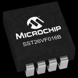
SST26VF016B-104I/MF
Serial 2.5V/3V 16Mbit 16M x 1bit 8ns/5ns 8-Pin WDFN EP
- RoHS 10 Compliant
- Tariff Charges
The Serial Quad I/O™ (SQI™) family of flash-memory devices features a six-wire, 4-bit I/O interface that allows for low-power, high-performance operation in a low pin-count package. SST26VF016B also support full command-set compatibility to traditional Serial Peripheral Interface (SPI) protocol. System designs using SQI flash devices occupy less board space and ultimately lower system costs. All members of the 26 Series, SQI family are manufactured with proprietary, high-performance CMOS SuperFlash® technology. The split-gate cell design and thickoxide tunneling injector attain better reliability and manufacturability compared with alternate approaches. The SST26VF016B significantly improve performance and reliability, while lowering power consumption. These devices write (Program or Erase) with a single power supply of 2.7-3.6V. The total energy consumed is a function of the applied voltage, current, and time of application. Since for any given voltage range, the SuperFlash technology uses less current to program and has a shorter erase time, the total energy consumed during any Erase or Program operation is less than alternative flash memory technologies. SST26VF016B is offered in 8-contact WDFN (6 mm x 5 mm), 8-lead SOIJ (208 mil), and 8-lead SOIC (150 mil). Two configurations are available upon order: SST26VF016B default at power-up has the WP# and Hold# pins enabled.
Single Voltage Read and Write Operations 2.7-3.6V Serial Interface Architecture Nibble-wide multiplexed I/O’s with SPI-like serial command structure Mode 0 and Mode 3 x1/x2/x4 Serial Peripheral Interface (SPI) Protocol High Speed Clock Frequency 104 MHz max Burst Modes Continuous linear burst 8/16/32/64 Byte linear burst with wrap-around Superior Reliability - Endurance: 100,000 Cycles (min) Greater than 100 years Data Retention Low Power Consumption: Active Read current: 15 mA (typical @ 104 MHz) - Standby Current: 15 µA (typical) Fast Erase Time Sector/Block Erase: 18 ms (typ), 25 ms (max) - Chip Erase: 35 ms (typ), 50 ms (max) Page-Program 256 Bytes per page in x1 or x4 mode End-of-Write Detection Software polling the BUSY bit in status register Flexible Erase Capability Uniform 4 KByte sectors Software Reset (RST) mode Software Write Protection Individual-Block Write Protection with permanent lock-down capability 64 KByte blocks, two 32 KByte blocks, and eig
Technical Attributes
Find Similar Parts
| Description | Value | |
|---|---|---|
| 8 ns | ||
| Sectored | ||
| Symmetrical | ||
| Yes | ||
| 104 MHz | ||
| 16 Mbit | ||
| No | ||
| Yes | ||
| WSON | ||
| Serial | ||
| Matte Tin | ||
| Bottom|Top | ||
| 260 | ||
| 0.05/Chip s | ||
| 20 mA | ||
| 1.5/Page ms | ||
| 8/5 ns | ||
| 16 Mbit | ||
| Surface Mount | ||
| MSL 1 - Unlimited | ||
| 8 | ||
| 1 Bit | ||
| 16 MWords | ||
| -40 to 85 °C | ||
| 125 °C | ||
| -40 °C | ||
| 8WDFN EP | ||
| 8 | ||
| 6 x 5 x 0.73 | ||
| 25 mA | ||
| 2.7 to 3.6 V | ||
| No | ||
| Industrial | ||
| No | ||
| WDFN EP | ||
| 3.6 V | ||
| 2.3 V | ||
| 3.3 V | ||
| 2.5, 3 V |
ECCN / UNSPSC / COO
| Description | Value |
|---|---|
| Country of Origin: | RECOVERY FEE |
| ECCN: | EAR99 |
| HTSN: | 8542320051 |
| Schedule B: | 8542320040 |
