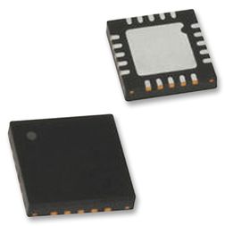
MIC68220YML-TR
LDO Regulator Pos 0.5V to 5.5V 2A 20-Pin MLF T/R
- RoHS 10 Compliant
- Tariff Charges
The MIC68220 is a dual high peak current LDO regulator designed specifically for powering applications such as FPGA core voltages that require high start up current with lower nominal operating current. Capable of sourcing 2A of current per channel for start-up, the MIC68220 provides high power from a small MLF™ leadless package. The MIC68220 can also implement a variety of power-up and power-down protocols such as sequencing, tracking, and ratiometric tracking. The MIC68220 operates from a wide input range of 1.65V to 5.5V, which includes all of the main supply voltages commonly available today. It is designed to drive digital circuits requiring low voltage at high currents (i.e. PLDs, DSP, microcontroller, etc.). The MIC68220 incorporates a delay pin (Delay) for control of power on reset output (POR) at turn-on and power-down delay at turn-off. In addition there is a ramp control pin (RC) for either tracking applications or output voltage slew rate adjustment at turnon. This is important in applications where the load is highly capacitive and in-rush currents can cause supply voltages to fail and microprocessors or other complex logic chips to hang up. The MIC68220’s can be configured in two modes. In tracking mode, the output voltage of Vout1 drives the RC2 pin so that the Vout2 tracks Vout1 during turn-on and turnoff. In sequencing mode, POR1 of Vout1 drives the enable pin (EN2) of Vout2 so that it turns on after the Vout1 and turns off before (or after) Vout1. This behavior is critical for power-up and power-down control in multi-output power supplies. The MIC68220 is fully protected offering both thermal and current limit protection, and reverse current protection. The MIC68220 has a junction temperature range of -40°C to +125°C and is available in an adjustable Vout1 & Vout2 version. The MIC68220 is offered in a low profile 4mm x 5mm 20ld MLF® package.
Stable with 4.7uF ceramic output capacitor Input voltage range: 1.65V to 5.5V 0.5V reference +1.0% initial output tolerance 2A maximum output current - peak start up 1A Continuous Operating Current Tracking on turn-on and turn-off with pin strapping Timing Controlled Sequencing On/Off Programmable Ramp Control™ for in-rush current limiting and slew rate control of the output voltage on Turn-On Power-on Reset (POR) supervisor with programmable delay time Single Master can control multiple Slave regulators with tracking output voltages Tiny 4mm x 5mm MLF® package Maximum dropout (VIN - VOUT) of 400mV over temperature at 1A output current Adjustable Output Voltages Excellent line and load regulation specifications Logic controlled shutdown Thermal shutdown and current limit protection
Technical Attributes
Find Similar Parts
| Description | Value | |
|---|---|---|
| 2 % | ||
| VDFN | ||
| 5.5 V | ||
| 1.65 V | ||
| 1.65 to 5.5 V | ||
| 44 °C/W | ||
| Gold over Nickel Palladium | ||
| 1 % | ||
| 0.6@2A V | ||
| 80 mA | ||
| Surface Mount | ||
| MSL 2 - 1 year | ||
| 2 | ||
| 20 | ||
| 2 | ||
| -40 to 125 °C | ||
| 125 °C | ||
| -40 °C | ||
| 2 A | ||
| Adjustable | ||
| 0.5 to 5.5 V | ||
| 20MLF | ||
| 20 | ||
| Positive | ||
| 5 x 4 x 0.8 mm | ||
| Adj 2A LDO Voltage Regulators | ||
| 0.5 V | ||
| Extended Industrial | ||
| MLF | ||
| 0.3@2A V |
ECCN / UNSPSC / COO
| Description | Value |
|---|---|
| Country of Origin: | RECOVERY FEE |
| ECCN: | EAR99 |
| HTSN: | 8542330001 |
| Schedule B: | 8542330000 |
