
LAN91C113-NS
Non PCI Ethernet Single Chip 128-Pin QFP
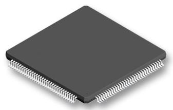
-
 RoHS 10 Compliant
 -
 Tariff Charges

The SMSC LAN91C113 is designed to fa cilitate the implementat ion of a third generati on of Fast Ethernet connectivity solutions for embedded applications. For this third generation of products, flexibility and integration dominate the design requirements. The LAN91C113 is a mixed signal Analog/ Digital device that implements the MAC and PHY portion of the CSMA/CD protocol at 10 and 100 Mbps. The design will also minimize data throughput constraints utilizing a 16-bit or 8-bit bus Host interface in embedded applications The total internal memory FIFO buffer size is 8 Kbytes , which is the total chip storage for transmit and receive operations. The SMSC LAN91C113 is software compatible with the LAN9000 family of products Memory management is handled using a patent ed optimized MMU (Memory Management Unit) architecture and a 16-bit wide inter nal data path. This I/O mapped archit ecture can sustain back-to-back frame transmission and reception for superior dat a throughput and optimal performance. It also dynamically allocates buffer memory in an efficient buffer utilization scheme, reducing software tasks and relieving the host CPU from performi ng these housekeeping functions. The SMSC 91C113 provides a flexible slave interfac e for easy connectivity with industry-standard buses. The Bus Interface Unit (BIU) can handle synchronous as well as asynchronous transfers, with different signals being used for each one. Asynchronous bus s upport for ISA is support ed even though ISA cannot sustain 100 Mbps traffic. Fast Ethernet data rates are attainable fo r ISA-based nodes on t he basis of the aggregate traffic benefit Two different interfaces are suppor ted on the network side. The firs t Interface is a standard Magnetics transmit/receive pair interfacing to 10/ 100Base-T utilizing the internal physica l layer block. The second interface follows the MII (Media Independent Interfac e) specification standard, consisting of 4 bit wide data transfers at the nibbl
- Single Chip Ethernet Controller
- Dual Speed - 10/100 Mbps
- Fully Supports Full Duplex Switched Ethernet
- 8 Kbytes Internal Memory for Receive and Transmit FIFO Buffers
- Enhanced Power Management Features
- Optional Configuration via Serial EEPROM Interface
- Supports 8, 16 Bit CPU Accesses
- Internal 16 Bit Wide Data Path (Into Packet Buffer Memory)
- Early TX, Early RX Functions
- Built-in Transparent Arbitration for Slave Sequential Access Architecture
- Flat MMU Architecture with Symmetric Transmit and Receive Structures and Queues
- 3.3V Operation with 5V Tolerant IO Buffers (See Pin List Description for Additional Details)
- Single 25 MHz Reference Clock for Both PHY and MAC
- External 25Mhz-output pin for an external PHY supporting PHYs physical media.
- Low Power CMOS Design
- Supports Multiple Embedded Processor Host Interfaces
- ARM
- SH
- Power PC
- Co
Technical Attributes
Find Similar Parts
| Description | Value | |
|---|---|---|
| Surface Mount | ||
| 128 | ||
| 0 to 85 °C | ||
| 85 °C | ||
| 0 °C | ||
| 128 | ||
| 20 x 14 x 3.05 mm | ||
| QFP | ||
| 3.3 V | ||
| Non PCI Ethernet Single Chip |
ECCN / UNSPSC / COO
| Description | Value |
|---|---|
| Country of Origin: | RECOVERY FEE |
| ECCN: | EAR99 |
| HTSN: | 8542310030 |
| Schedule B: | 8542310055 |
 Factory Lead Time: