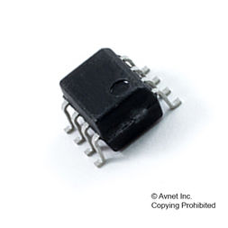
MX25L6436EM2I-10G
MCXMX25L6436EM2I-10G
- RoHS 10 Compliant
- Tariff Charges
The MX25L6436E is 67,108,864 bits serial Flash memory, which is configured as 8,388,608 x 8 internally. When it is in two or four I/O mode, the structure becomes 33,554,432 bits x 2 or 16,777,216 bits x 4. The MX25L6436E features a serial peripheral interface and software protocol allowing operation on a simple 3-wire bus. The three bus signals are a clock input (SCLK), a serial data input (SI), and a serial data output (SO). Serial access to the device is enabled by CS# input.
The MX25L6436E provides high performance read mode, which may latch address and data on both rising and falling edge of clock. By using this high performance read mode, the data throughput may be doubling. Moreover, the performance may reach direct code execution, the RAM size of the system may be reduced and further saving system cost.
The MX25L6436E, MXSMIOTM (Serial Multi I/O) flash memory, provides sequential read operation on the whole chip and multi-I/O features.
When it is in dual I/O mode, the SI pin and SO pin become SIO0 pin and SIO1 pin for address/dummy bits input and data output. When it is in quad I/O mode, the SI pin, SO pin, WP# pin and NC pin become SIO0 pin, SIO1 pin, SIO2 pin and SIO3 pin for address/dummy bits input and data Input/Output.
After program/erase command is issued, auto program/erase algorithms which program/erase and verify the specified page or sector/block locations will be executed. Program command is executed on byte basis, or page (256 bytes) basis, or word basis. Continuously Program mode and erase command are executed on 4K-byte sector, 32Kbyte/64K-byte block, or whole chip basis.
To provide user with ease of interface, a status register is included to indicate the status of the chip. The status read command can be issued to detect completion status of a program or erase operation via the WIP bit.
When the device is not in operation and CS# is high, it is put in standby mode and draws less than 100uA DC current.
- 67,108,864 bit serial flash memory
- Serial Peripheral Interface (SPI) compatible - Mode 0 and Mode 3
- 64Mb: 67,108,864 x 1 bit structure or 33,554,432 x 2 bits (two I/O mode) structure or 16,777,216 x 4 bits (four I/O mode) structure
- 2048 Equal Sectors with 4K bytes each
- Any Sector can be erased individually
- 256 Equal Blocks with 32K bytes each
- Any Block can be erased individually
- 128 Equal Blocks with 64K bytes each
- Any Block can be erased individually
- Power Supply Operation
- 2.7 to 3.6 volt for read, erase, and program operations
- Latch-up protected to 100mA from -1V to Vcc +1V
Technical Attributes
Find Similar Parts
| Description | Value | |
|---|---|---|
| 12 ns | ||
| Sectored | ||
| Symmetrical | ||
| No | ||
| NOR | ||
| 104 MHz | ||
| 64 MB | ||
| No | ||
| No | ||
| Serial-SPI | ||
| SPI | ||
| 80/Chip s | ||
| 22 mA | ||
| 5/Page ms | ||
| 12 ns | ||
| 64 Mbit | ||
| Surface Mount | ||
| 1, 2, 4 Bit | ||
| 64, 32, 16 MWords | ||
| -40 to 85 °C | ||
| 85 °C | ||
| -40 °C | ||
| 8SOP | ||
| 25 mA | ||
| 0 | ||
| Industrial | ||
| No | ||
| 3.3 V | ||
| 3.3000 V |
ECCN / UNSPSC / COO
| Description | Value |
|---|---|
| Country of Origin: | RECOVERY FEE |
| ECCN: | 3A991.B.1.A |
| HTSN: | 8542320071 |
| Schedule B: | 8542320040 |
