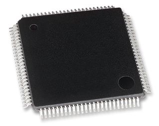
IS61NLP12832A-200TQLI
SRAM Chip Sync Quad 3.3V 4M-Bit 128K x 32 3.1ns 100-Pin TQFP
The 4 Meg feature high-speed, low-power synchronous static RAMs designed to provide a burstable, high-performance, 'no wait' state, device for networking and communications applications. They are organized as 128K words by 32 bits fabricated with advanced CMOS technology. Incorporating a 'no wait' state feature, wait cycles are eliminated when the bus switches from read to write, or write to read. This device integrates a 2-bit burst counter, high-speed SRAM core, and high-drive capability outputs into a single monolithic circuit. All synchronous inputs pass through registers are controlled by a positive-edge-triggered single clock input. Operations may be suspended and all synchronous inputs ignored when Clock Enable, CKE is HIGH. In this state the internal device will hold their previous values. All Read, Write and Deselect cycles are initiated by the ADV input. When the ADV is HIGH the internal burst counter is incremented. New external addresses can be loaded when ADV is LOW. Write cycles are internally self-timed and are initiated by the rising edge of the clock inputs and when WE is LOW. Separate byte enables allow individual bytes to be written. A burst mode pin (MODE) defines the order of the burst sequence. When tied HIGH, the interleaved burst sequence is selected. When tied LOW, the linear burst sequence is selected.
- 100 percent bus utilization
- No wait cycles between Read and Write
- Internal self-timed write cycle
- Individual Byte Write Control
- Single R/W (Read/Write) control pin
- Clock controlled, registered address, data and control
- Interleaved or linear burst sequence control using MODE input
- Three chip enables for simple depth expansion and address pipelining
- Power Down mode
- Common data inputs and data outputs
- CKE pin to enable clock and suspend operation
- JEDEC 100-pin TQFP, 165-ball PBGA and 119- ball PBGA packages
- Power supply: Vdd 3.3V (± 5%), Vddq 3.3V/2.5V (± 5%)
- Industrial temperature available
- Lead-free available
Technical Attributes
Find Similar Parts
| Description | Value | |
|---|---|---|
| 17 Bit | ||
| Pipelined | ||
| 200 MHz | ||
| 4 Mbit | ||
| Matte Tin | ||
| 260 °C | ||
| 200 MHz | ||
| 250 mA | ||
| 3.1 ns | ||
| 4 Mbit | ||
| Surface Mount | ||
| MSL 3 - 168 hours | ||
| 100 | ||
| 32 Bit | ||
| 32 Bit | ||
| 4 | ||
| 128 kWords | ||
| -40 to 85 °C | ||
| 85 °C | ||
| -40 °C | ||
| 100TQFP | ||
| 100 | ||
| 20.10 x 14.1 x 1.45 mm | ||
| 0 | ||
| Industrial | ||
| TQFP | ||
| 3.3 V | ||
| 3.3000 V |
ECCN / UNSPSC / COO
| Description | Value |
|---|---|
| Country of Origin: | RECOVERY FEE |
| ECCN: | 3A991.B.2.A |
| HTSN: | 8542320041 |
| Schedule B: | 8542320040 |
