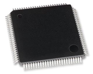
IS61LPS51236A-200TQLI
SRAM Chip Sync Quad 3.3V 18M-Bit 512K x 36 3.1ns 100-Pin TQFP
The ISSI IS61LPS51236A is high-speed, low-powersynchronous static RAMs designed to provide burstable,high-performance memory for communication and networkingapplications. The IS61LPS/VPS51236A is organizedas 524,288 words by 36 bits, the IS61LPS/VPS102418A isorganized as 1,048,576words by 18 bits, and the IS61LPS/VPS25672A is organized as 262,144 words by 72 bits.Fabricated with ISSI's advanced CMOS technology, thedevice integrates a 2-bit burst counter, high-speed SRAMcore, and high-drive capability outputs into a single monolithiccircuit. All synchronous inputs pass through registerscontrolled by a positive-edge-triggered single clock input. Write cycles are internally self-timed and are initiated bythe rising edge of the clock input.Write cycles can be oneto four bytes wide as controlled by the write control inputs.Separate byte enables allow individual bytes to be written.Thebytewriteoperationisperformedbyusingthebytewriteenable (BWE)\ input combined with one or more individualbyte write signals (BWx)\. In addition, Global Write (GW)\is available for writing all bytes at one time, regardless ofthe byte write controls. Bursts can be initiated with either ADSP\ (Address StatusProcessor) or ADSC\ (Address Status Cache Controller)input pins. Subsequent burst addresses can be generatedinternally and controlled by the ADV\ (burst addressadvance) input pin. The mode pin is used to select the burst sequence order,Linearburstisachievedwhenthispinis tiedLOW.Interleaveburst is achieved when this pin is tied HIGH or left floating.
- Internal self-timed write cycle
- Individual Byte Write Control and Global Write
- Clock controlled, registered address, data and control
- Burst sequence control using MODE input
- Three chip enable option for simple depth expansion and address pipelining
- Common data inputs and data outputs
- Auto Power-down during deselect
- Single cycle deselect
- Snooze MODE for reduced-power standby
- JTAG Boundary Scan for PBGA package
- Power Supply LPS: Vdd 3.3V + 5%, Vddq 3.3V/2.5V + 5% VPS: Vdd 2.5V + 5%, Vddq 2.5V + 5%
- JEDEC 100-Pin TQFP, 119-ball PBGA, 165-ball PBGA, and 209-ball (x72) packages
- Lead-free available
Technical Attributes
Find Similar Parts
| Description | Value | |
|---|---|---|
| 19 Bit | ||
| Pipelined | ||
| 200 MHz | ||
| SDR | ||
| 18 Mbit | ||
| Matte Tin | ||
| 260 | ||
| 200 MHz | ||
| 475 mA | ||
| 3.1 ns | ||
| 18 Mbit | ||
| Surface Mount | ||
| MSL 3 - 168 hours | ||
| 100 | ||
| 36 Bit | ||
| 36 Bit | ||
| 4 | ||
| 512 kWords | ||
| -40 to 85 °C | ||
| 85 °C | ||
| -40 °C | ||
| 100TQFP | ||
| 100 | ||
| 20.1 x 14.1 x 1.45 mm | ||
| No | ||
| Industrial | ||
| TQFP | ||
| 3.465 V | ||
| 3.135 V | ||
| 3.3 V | ||
| Synchronous | ||
| 3.3000 V |
ECCN / UNSPSC / COO
| Description | Value |
|---|---|
| Country of Origin: | RECOVERY FEE |
| ECCN: | 3A991.B.2.A |
| HTSN: | 8542320041 |
| Schedule B: | 8542320040 |
