
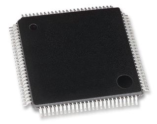
IS61LF6436A-8.5TQLI-TR
SRAM Chip Sync Quad 2.5V/3.3V 2M-Bit 64K x 36 8.5ns 100-Pin TQFP T/R


The IS61LF6436A are high-speed, low-power synchronous static RAM designed to provide a burstable, high-performance, memory. The device is organized as 65,536 words by 36 bits. They are fabricated advanced CMOS technology. The device integrates a 2-bit burst counter, high-speed SRAM core, and high-drive capability outputs into a single monolithic circuit. All synchronous inputs pass through registers controlled by a positive-edge-triggered single clock input. Write cycles are internally self-timed and are initiated by the rising edge of the clock input. Write cycles can be from one to four bytes wide as controlled by the write control inputs. Separate byte enables allow individual bytes to be written. BWa\ controls DQa, BWb\ controls DQb, BWc\ controls DQc, BWd\ controls DQd, conditioned by BWE\ being LOW. A LOW on GW\ input would cause all bytes to be written. Bursts can be initiated with either ADSP\ (Address Status Processor) or ADSC\ (Address Status Cache Controller) input pins. Subsequent burst addresses can be generated internally by the IS61LF6436A and controlled by the ADV\ (burst address advance) input pin. The mode pin is used to select the burst sequence order. Linear burst is achieved when this pin is tied LOW. Interleave burst is achieved when this pin is tied HIGH or left floating.
- Internal self-timed write cycle
- Individual Byte Write Control and Global Write
- Clock controlled, registered address, data and control
- Interleaved or linear burst sequence control using MODE input
- Three chip enables for simple depth expansion and address pipelining
- Common data inputs and data outputs
- Power-down control by ZZ input
- JEDEC 100-Pin TQFP package
- Power Supply: +3.3V or 2.5V Vddq
- Control pins mode upon power-up:
- MODE in interleave burst mode
- ZZ in normal operation mode
- Industrial Temperature Available: (-40°C to +85°C)
- Lead-free available
Technical Attributes
Find Similar Parts
| Description | Value | |
|---|---|---|
| 16 Bit | ||
| Flow-Through | ||
| 90 MHz | ||
| SDR | ||
| 2 Mbit | ||
| Matte Tin | ||
| 260 °C | ||
| 90 MHz | ||
| 150 mA | ||
| 2.625, 3.63 V | ||
| 8.5 ns | ||
| 2 Mbit | ||
| 2.375, 3.135 V | ||
| Surface Mount | ||
| MSL 3 - 168 hours | ||
| 100 | ||
| 36 Bit | ||
| 36 Bit | ||
| 4 | ||
| 64 kWords | ||
| -40 to 85 °C | ||
| 85 °C | ||
| -40 °C | ||
| 100TQFP | ||
| 100 | ||
| 20 x 14 x 1.4 mm | ||
| No | ||
| Industrial | ||
| Synchronous SRAM | ||
| TQFP | ||
| 2.625, 3.63 V | ||
| 2.375, 3.135 V | ||
| 2.5, 3.3 V | ||
| Synchronous | ||
| 2.5, 3.3 V |
ECCN / UNSPSC / COO
| Description | Value |
|---|---|
| Country of Origin: | RECOVERY FEE |
| ECCN: | 3A991.B.2.A |
| HTSN: | 8542320041 |
| Schedule B: | 8542320040 |