
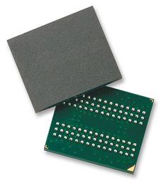
IS43LR32160C-6BLI
DRAM Chip Mobile DDR SDRAM 512M-Bit 16M x 32 1.8V 90-Pin TFBGA


The IS43LR32160C-6BLI is a 536870912-bit CMOS Mobile Double Data Rate Synchronous DRAM organized as 4 banks of 4194304 words x 32-bit. This product uses a double-data-rate architecture to achieve high-speed operation. The data input/output signals are transmitted on a 32-bit bus. The double data rate architecture is essentially a 2N pre-fetch architecture with an interface designed to transfer two data words per clock cycle at the I/O pins. This product offers fully synchronous operations referenced to both rising and falling edges of the clock. The data paths are internally pipelined and 2n-bit pre-fetched to achieve very high bandwidth. All input and output voltage levels are compatible with LVCMOS.
- JEDEC standard 1.8V power supply
- 4-Internal banks for concurrent operation
- MRS cycle with address key programs
- Fully differential clock inputs
- All inputs except data & DM are sampled at the rising edge of the system clock
- Data I/O transaction on both edges of data strobe
- Bidirectional data strobe per byte of data
- DM for write masking only
- Edge aligned data and data strobe output
- Center aligned data and data strobe input
Technical Attributes
Find Similar Parts
| Description | Value | |
|---|---|---|
| 13 Bit | ||
| 166 MHz | ||
| 32 Bit | ||
| 512 Mbit | ||
| Mobile DDR SDRAM | ||
| Tin-Silver-Copper | ||
| 260 °C | ||
| 166 MHz | ||
| 60 mA | ||
| 5.5|8 ns | ||
| 512 Mbit | ||
| Surface Mount | ||
| MSL 3 - 168 hours | ||
| 90 | ||
| 4 | ||
| 32 Bit | ||
| 32 Bit | ||
| 1.8000 V | ||
| -40 to 85 °C | ||
| 85 °C | ||
| -40 °C | ||
| 16M x 32 | ||
| 90TFBGA | ||
| 90 | ||
| Industrial | ||
| TFBGA | ||
| 1.8 V | ||
| Mobile DDR SDRAM |
ECCN / UNSPSC / COO
| Description | Value |
|---|---|
| Country of Origin: | RECOVERY FEE |
| ECCN: | EAR99 |
| HTSN: | 8542320028 |
| Schedule B: | 8542320015 |