
S25FL512SDPMFIG11
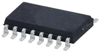
NOR Flash Serial-SPI 3V 512Mbit 512M x 1bit 8ns 16-Pin SOIC Tube
-
 RoHS 10 Compliant
 -
 Tariff Charges

The Spansion S25FL512S device is a flash non-volatile memory product using: MirrorBit technology - that stores two data bits in each memory array transistor Eclipse architecture - that dramatically improves program and erase performance 65 nm process lithography This device connects to a host system via a Serial Peripheral Interface (SPI). Traditional SPI single bit serial input and output (Single I/O or SIO) is supported as well as optional two bit (Dual I/O or DIO) and four bit (Quad I/O or QIO) serial commands. This multiple width interface is called SPI Multi-I/O or MIO. In addition, the FL-S family adds support for Double Data Rate (DDR) read commands for SIO, DIO, and QIO that transfer address and read data on both edges of the clock. The Eclipse architecture features a Page Programming Buffer that allows up to 256 words (512 bytes) to be programmed in one operation, resulting in faster effective programming and erase than prior generation SPI program or erase algorithms. Executing code directly from flash memory is often called Execute-In-Place or XIP. By using FL-S devices at the higher clock rates supported, with QIO or DDR-QIO commands, the instruction read transfer rate can match or exceed traditional parallel interface, asynchronous, NOR flash memories while reducing signal count dramatically. The S25FL512S product offers high densities coupled with the flexibility and fast performance required by a variety of embedded applications. It is ideal for code shadowing, XIP, and data storage.
- Density
- 512 Mbits (64 Mbytes)
- Serial Peripheral Interface (SPI)
- SPI Clock polarity and phase modes 0 and 3
- Double Data Rate (DDR) option
- Extended Addressing: 32-bit address
- Serial Command set and footprint compatible with S25FL-A, S25FL-K, and S25FL-P SPI families
- Multi I/O Command set and footprint compatible with S25FL-P SPI family
- READ Commands
- Normal, Fast, Dual, Quad, Fast DDR, Dual DDR, Quad DDR
- AutoBoot - power up or reset and execute a Normal or Quad read command automatically at a preselected address
- Common Flash Interface (CFI) data for configuration information.
- Programming (1.5 Mbytes/s)
- 512-byte Page Programming buffer
- Quad-Input Page Programming (QPP) for slow clock systems
- Erase (0.5 to 0.65 Mbytes/s)
- Uniform 256-kbyte sectors
- Cycling Endurance
- 100,000 Program-Erase Cycles
Technical Attributes
Find Similar Parts
| Description | Value | |
|---|---|---|
| 14.5 ns | ||
| 66 MHz | ||
| Serial NOR | ||
| SOIC | ||
| Surface Mount | ||
| CFI, QSPI | ||
| 64M x 8bit | ||
| 512 Mbit | ||
| 16 | ||
| 85 °C | ||
| -40 °C | ||
| 3V Serial NOR Flash Memories | ||
| 3.6 V | ||
| 2.7 V | ||
| 3 V |
ECCN / UNSPSC / COO
| Description | Value |
|---|---|
| Country of Origin: | NO RECOVERY FEE |
| ECCN: | 3A991B1A |
| HTSN: | 8542320071 |
| Schedule B: | 8542320070 |
 Factory Lead Time: