
S25FL256SDPMFV000
Click image to enlarge
Manufacturer:Infineon
Product Category:
Memory, Flash Memory
Avnet Manufacturer Part #: S25FL256SDPMFV000
Secondary Manufacturer Part#: S25FL256SDPMFV000
-
 RoHS 10 Compliant
 -
 Tariff Charges
Technical Attributes
Find Similar Parts
| Description | Value | |
|---|---|---|
| 8 ns | ||
| 32 Bit | ||
| Sectored | ||
| Symmetrical | ||
| Yes | ||
| NOR | ||
| 66 MHz | ||
| 256 Mbit | ||
| No | ||
| Yes | ||
| Serial-SPI | ||
| SPI | ||
| Tin | ||
| Bottom|Top | ||
| 260 | ||
| 330/Chip s | ||
| 75 mA | ||
| 0.75/Page ms | ||
| 8 ns | ||
| 256 Mbit | ||
| Surface Mount | ||
| MSL 3 - 168 hours | ||
| 16 | ||
| 1 Bit | ||
| 256 MWords | ||
| -40 to 105 °C | ||
| 105 °C | ||
| -40 °C | ||
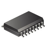
| 16SOIC | ||
| 16 | ||
| 10.3 x 7.5 x 2.55(Max) | ||
| 100 mA | ||
| 2.7 to 3.6 V | ||
| No | ||
| Automotive | ||
| No | ||
| SOIC | ||
| 3 V | ||
| 3.0000 V |
ECCN / UNSPSC / COO
| Description | Value |
|---|---|
| Country of Origin: | NO RECOVERY FEE |
| ECCN: | 3A991B1A |
| HTSN: | 8542320071 |
| Schedule B: | 8542320070 |