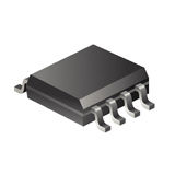
S25FL032P0XMFI010
NOR Flash Serial-SPI 3V/3.3V 32Mbit 4M x 8bit 8ns 8-Pin SOIC W Tray
- RoHS 10 Compliant
- Tariff Charges
The S25FL032P0XMFI010 is a 32MB single-power-supply CMOS Flash Memory with 104MHz SPI (serial peripheral interface) multi I/O bus. The device consists of 64 uniform 64kB sectors with the two 64kB sectors further split up into thirty-two 4kB sub sectors. The S25FL032P device is fully backward compatible with the S25FL032A device. The device accepts data written to SI (serial input) and outputs data on SO (serial output). The device is designed to be programmed in-system with the standard system 3VCC supply. The memory can be programmed 1 to 256 bytes at a time, using the page program command. The device supports sector erase and bulk erase commands. Each device requires only a 3V power supply for both read and write functions. Internally generated and regulated voltages are provided for the program operations. This device requires a high voltage supply to the W#/ACC pin to enable the accelerated programming mode.
- Dual output read using both SI and SO pins as output pins at a clock rate of up to 80MHz
- Single power supply operation
- Memory architecture
- Program operations are on a page by page basis
- Quad page programming
- Bulk erase function
- Cycling endurance - 100000 cycles per sector typical
- Data retention - 20 years typical
- Device ID - JEDEC standard two-byte electronic signature
- Process technology - manufactured on 0.09µm MirrorBit® process technology
Technical Attributes
Find Similar Parts
| Description | Value | |
|---|---|---|
| 8 ns | ||
| 1 Bit | ||
| Sectored | ||
| Symmetrical | ||
| No | ||
| NOR | ||
| 104 MHz | ||
| 32 Mbit | ||
| No | ||
| No | ||
| NOR | ||
| SOIC W | ||
| Surface Mount | ||
| Serial (SPI) | ||
| SPI | ||
| Matte Tin | ||
| Bottom|Top | ||
| 260 | ||
| 64/Chip s | ||
| 38 mA | ||
| 3/Page ms | ||
| 8 ns | ||
| 4M x 8bit | ||
| 32 Mbit | ||
| Surface Mount | ||
| MSL 3 - 168 hours | ||
| 8 | ||
| 8 Bit | ||
| 4 MWords | ||
| -40 to 85 °C | ||
| 85 °C | ||
| -40 °C | ||
| 8SOIC W | ||
| 8 | ||
| 5.28 x 5.28 x 1.91 mm | ||
| 3V Serial NOR Flash Memories | ||
| 26 mA | ||
| 2.7 to 3.6 V | ||
| No | ||
| Industrial | ||
| No | ||
| SOIC W | ||
| 3.6 V | ||
| 2.7 V | ||
| 3, 3.3 V | ||
| 3, 3.3 V |
ECCN / UNSPSC / COO
| Description | Value |
|---|---|
| Country of Origin: | RECOVERY FEE |
| ECCN: | 3A991.B.1.A |
| HTSN: | 8542320071 |
| Schedule B: | 8542320070 |
