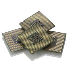
CY7C1570KV18-400BZXC
SRAM Chip Sync Single 1.8V 72M-Bit 2M x 36 0.45ns 165-Pin FBGA
The CY7C1570KV18 is 1.8V Synchronous Pipelined SRAMs equipped with DDR-II+ architecture. The DDR-II+ consists of an SRAM core with advanced synchronous peripheral circuitry. Addresses for read and write are latched on alternate rising edges of the input (K) clock. Write data is registered on the rising edges of both K and K. Read data is driven on the rising edges of K and K. Each address location is associated with 36-bit words (CY7C1570KV18) that burst sequentially into or out of the device. Asynchronous inputs include an output impedance matching input (ZQ). Synchronous data outputs (Q, sharing the same physical pins as the data inputs D) are tightly matched to the two output echo clocks CQ/CQ, eliminating the need for separately capturing data from each individual DDR SRAM in the system design. All synchronous inputs pass through input registers controlled by the K or K input clocks. All data outputs pass through output registers controlled by the K or K input clocks. Writes are conducted with on-chip synchronous self-timed write circuitry.
- 72 Mbit density (8M x 8, 8M x 9, 4M x 18, 2M x 36)
- 550 MHz clock for high bandwidth
- 2-word burst for reducing address bus frequency
- Double Data Rate (DDR) interfaces (data transferred at 1100 MHz) at 550 MHz
- Available in 2.5 clock cycle latency
- Two input clocks (K and K) for precise DDR timing
- SRAM uses rising edges only
- Echo clocks (CQ and CQ) simplify data capture in high-speed systems
- Data valid pin (QVLD) to indicate valid data on the output
- Synchronous internally self-timed writes
- DDR-II+ operates with 2.5 cycle read latency when DOFF is asserted HIGH
- Operates similar to DDR-I device with 1 cycle read latency when DOFF is asserted LOW
- Core VDD = 1.8V ± 0.1V; IO VDDQ = 1.4V to VDD[1]
- Supports both 1.5V and 1.8V IO supply
- HSTL inputs and variable drive HSTL output buffers
- Available in 165-Ball FBGA package (13 x 15 x 1.4 mm)
- Off
Technical Attributes
Find Similar Parts
| Description | Value |
|---|
ECCN / UNSPSC / COO
| Description | Value |
|---|---|
| Country of Origin: | RECOVERY FEE |
| ECCN: | 3A991.B.2.B |
| HTSN: | 8542320041 |
| Schedule B: | 8542320040 |
