
CY7C1444KV33-250AXC
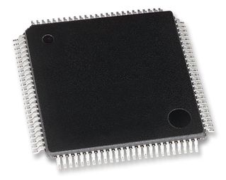
SRAM Chip Sync Quad 3.3V 36M-Bit 1M x 36 2.5ns 100-Pin TQFP Tray


The CY7C1444KV33 SRAMs integrate 1M × 36 SRAM cells with advanced synchronous peripheral circuitry and a two-bit counter for internal burst operation. All synchronous inputs are gated by registers controlled by a positive-edge-triggered clock (CLK) input. The synchronous inputs include all addresses, all data inputs, address-pipelining chip enable (CE1\), depth-expansion chip enables (CE2 and CE3\), burst control inputs (ADSC\, ADSP\, and ADV\), write enables (BWX\, and BWE\), and global write (GW\). Asynchronous inputs include the output enable (OE\) and the ZZ pin.Addresses and chip enables are registered at rising edge of clock when either address strobe processor (ADSP\) or address strobe controller (ADSC\) are active. Subsequent burst addresses can be internally generated as controlled by the advance pin (ADV\).Address, data inputs, and write controls are registered on-chip to initiate a self-timed write cycle. This part supports byte write operations. Write cycles can be one to four bytes wide as controlled by the byte write control inputs. GW\ active LOW causes all bytes to be written. This device incorporates an additional pipelined enable register which delays turning off the output buffers an additional cycle when a deselect is executed. This feature allows depth expansion without penalizing system performance.The CY7C1444KV33 SRAMs operate from a +3.3 V core power supply while all outputs operate with a +3.3 V or a +2.5 V supply. All inputs and outputs are JEDEC-standard JESD8-5-compatible.
- Supports bus operation up to 250 MHz
- Available speed grades is 250 MHz
- Registered inputs and outputs for pipelined operation
- Optimal for performance (double-cycle deselect)
- Depth expansion without wait state
- 3.3-V core power supply
- 2.5-V or 3.3-V I/O power supply
- Fast clock-to-output times
- 2.5 ns (for 250-MHz device)
- Provide high-performance 3-1-1-1 access rate
- User-selectable burst counter supporting interleaved or linear burst sequences
- Separate processor and controller address strobes
- Synchronous self-timed writes
- Asynchronous output enable
- CY7C1444KV33 available in JEDEC-standard Pb-free 100-pin TQFP packages
- “ZZ” sleep mode option
Technical Attributes
Find Similar Parts
| Description | Value | |
|---|---|---|
| 20 Bit | ||
| 250 MHz | ||
| 36 Mbit | ||
| Gold over Nickel Palladium | ||
| 260 | ||
| 250 MHz | ||
| 240 mA | ||
| 2.5 ns | ||
| 36 Mbit | ||
| Surface Mount | ||
| MSL 3 - 168 hours | ||
| 100 | ||
| 36 Bit | ||
| 36 Bit | ||
| 4 | ||
| 1 MWords | ||
| 0 to 70 °C | ||
| 70 °C | ||
| 0 °C | ||
| 100TQFP | ||
| 100 | ||
| 14 x 20 x 1.4 | ||
| No | ||
| Commercial | ||
| TQFP | ||
| 3.63 V | ||
| 3.135 V | ||
| 3.3 V | ||
| 3.3000 V |
ECCN / UNSPSC / COO
| Description | Value |
|---|---|
| Country of Origin: | RECOVERY FEE |
| ECCN: | 3A991.B.2.B |
| HTSN: | 8542320041 |
| Schedule B: | 8542320040 |