
CY7C1371KV33-100AXC
SRAM Chip Sync Single 3.3V 18M-Bit 512K x 36 8.5ns 100-Pin TQFP Tray
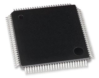


The CY7C1371KV33 is a 3.3 V, 512K × 36/1M × 18 synchronous flow through burst SRAM designed specifically to support unlimited true back-to-back read/write operations with no wait state insertion. The CY7C1371KV33 devices are equipped with the advanced No Bus Latency (NoBL) logic required to enable consecutive read/write operations with data being transferred on every clock cycle. This feature dramatically improves the throughput of data through the SRAM, especially in systems that require frequent write-read transitions.
All synchronous inputs pass through input registers controlled by the rising edge of the clock. The clock input is qualified by the clock enable signal, which when deasserted suspends operation and extends the previous clock cycle. Maximum access delay from the clock rise is 6.5 ns (133-MHz device).Write operations are controlled by the two or four byte write select and a write enable input. All writes are conducted with on-chip synchronous self-timed write circuitry.
Three synchronous chip enables and an asynchronous output enable (OE) provide for easy bank selection and output tristate control. To avoid bus contention, the output drivers are synchronously tristated during the data portion of a write sequence.
- No Bus Latency? (NoBL?) architecture eliminates dead cycles between write and read cycles
- Supports up to 133-MHz bus operations with zero wait states
- Data is transferred on every clock
- Pin-compatible and functionally equivalent to ZBT devices
- Registered inputs for flow through operation
- Byte write capability
- 3.3 V/2.5V I/O power supply (VDDQ)
- Fast clock-to-output times
- 6.5 ns (for 133-MHz device)
- Clock enable pin to enable clock and suspend operation
- Synchronous self-timed writes
- Asynchronous output enable
- Available in JEDEC-standard Pb-free 100-pin TQFP packages
- Three chip enables for simple depth expansion
- Automatic power-down feature available using ZZ mode or CE deselect
- Burst capability – linear or interleaved burst order
- Low standby power
- On chip Error Correction Code (ECC) to reduce Soft Error Rate (SER)
Technical Attributes
Find Similar Parts
| Description | Value |
|---|
ECCN / UNSPSC / COO
| Description | Value |
|---|---|
| Country of Origin: | RECOVERY FEE |
| ECCN: | 3A991.B.2.B |
| HTSN: | 8542320041 |
| Schedule B: | 8542320040 |
 Factory Lead Time: