
CY7C1356C-250AXCT
SRAM Chip Sync Dual 3.3V 9M-Bit 512K x 18 2.8ns 100-Pin TQFP T/R
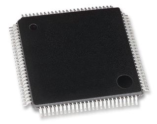


The CY7C1356C is 3.3V, 256 K × 36/512 K × 18 synchronous pipelined burst SRAMs with No Bus Latency (NoBL logic, respectively. They are designed to support unlimited true back-to-back read/write operations with no wait states. The CY7C1354C/CY7C1356C are equipped with the advanced (NoBL) logic required to enable consecutive read/write operations with data being transferred on every clock cycle. This feature greatly improves the throughput of data in systems that require frequent write/read transitions. The CY7C1354C/CY7C1356C are pin compatible and functionally equivalent to ZBT devices.
- Pin-compatible and functionally equivalent to ZBT
- Supports 250 MHz bus operations with zero wait states
- Available speed grades are 250, 200, and 166 MHz
- Internally self-timed output buffer control to eliminate the need to use asynchronous
- Fully registered (inputs and outputs) for pipelined operation
- Byte write capability
- Single 3.3 V power supply (VDD)
- 3.3 V or 2.5 V I/O power supply (VDDQ)
- Fast clock-to-output times
- 2.8 ns (for 250 MHz device)
- Clock enable (CE/ and OE/?) pin to suspend operation
- Synchronous self-timed writes
- Available in Pb-free 100-pin TQFP package, Pb-free, and non Pb-free 119-ball BGA package and 165-ball FBGA package
- IEEE 1149.1 JTAG-compatible boundary scan
- Burst capability - linear or interleaved burst order
- “ZZ” sleep mode option and stop clock option
Technical Attributes
Find Similar Parts
| Description | Value | |
|---|---|---|
| 250 MHz | ||
| 9 Mbit | ||
| 100 | ||
| 70 °C | ||
| 0 °C | ||
| 3.3 V |
ECCN / UNSPSC / COO
| Description | Value |
|---|---|
| Country of Origin: | NO RECOVERY FEE |
| ECCN: | 3A991.B.2.B |
| HTSN: | 8542320041 |
| Schedule B: | 8542320040 |
 Factory Lead Time: