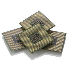
CY7C1321KV18-250BZC
SRAM Chip Sync Single 1.8V 18M-Bit 512K x 36 0.45ns 165-Pin FBGA Tray
CY7C1321KV18 is 1.8 V Synchronous Pipelined SRAMs equipped with DDR II architecture. The DDR II consists of an SRAM core with advanced synchronous peripheral circuitry and a two-bit burst counter. Addresses for read and write are latched on alternate rising edges of the input (K) clock. Write data is registered on the rising edges of both K and K. Read data is driven on the rising edges of C and C if provided, or on the rising edge of K and K if C/C are not provided. For CY7C1319KV18 and CY7C1321KV18, the burst counter takes in the least two significant bits of the external address and bursts four 18-bit words in the case of CY7C1319KV18, and four 36-bit words in the case of CY7C1321KV18, sequentially into or out of the device.
- 18-Mbit density (1 M × 18, 512 K × 36)
- 333-MHz clock for high bandwidth
- Four-word burst for reducing address bus frequency
- Double data rate (DDR) interfaces (data transferred at 666 MHz) at 333 MHz
- Two input clocks (K and K) for precise DDR timing
- SRAM uses rising edges only
- Two input clocks for output data (C and C) to minimize clock skew and flight time mismatches
- Echo clocks (CQ and CQ) simplify data capture in high speed systems
- Synchronous internally self-timed writes
- DDR II operates with 1.5 cycle read latency when DOFF is asserted HIGH
- Operates similar to DDR I device with one cycle read latency when DOFF is asserted LOW
- 1.8 V core power supply with HSTL inputs and outputs
- Variable drive HSTL output buffers
- Expanded HSTL output voltage (1.4 V-VDD)
- Supports both 1.5 V and 1.8 V I/O supply
- Available in 165-ball FBGA package (13 × 15
Technical Attributes
Find Similar Parts
| Description | Value |
|---|
ECCN / UNSPSC / COO
| Description | Value |
|---|---|
| Country of Origin: | RECOVERY FEE |
| ECCN: | 3A991.B.2.B |
| HTSN: | 8542320041 |
| Schedule B: | 8542320040 |
