
CY2305CSXC-1
Clock Buffer, Zero Delay, 10 MHz to 133 MHz, 5 Outputs, 3 V to 3.6 V, 8 Pins, SOIC
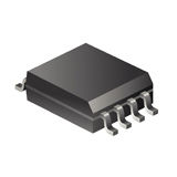
-
 RoHS 10 Compliant
 -
 Tariff Charges

CY2305CSXC-1 is a low-cost 3.3V zero delay buffer designed to distribute high speed clocks and is available in a 16-pin SOIC package. The CY2305C is an 8-pin version of the CY2309C. It accepts one reference input and drives out five low-skew clocks. It has on-chip phase locked loops (PLLs) which lock to an input clock on the REF pin. The PLL feedback is on-chip and is obtained from the CLKOUT pad. The CY2309C has two banks of four outputs each that are controlled by the select inputs. If all output clocks are not required, Bank B is three-stated. The input clock is directly applied to the outputs by the select inputs for chip and system testing purposes.
- 5-output zero delay buffer
- Zero input and output propagation delay
- Multiple low skew outputs
- 50ps typical cycle-to-cycle jitter (15pF, 66MHz)
- Standard drive
- Available in 8 pin SOIC package
Technical Attributes
Find Similar Parts
| Description | Value | |
|---|---|---|
| Zero Delay Buffer | ||
| 133 MHz | ||
| 10 MHz | ||
| LVCMOS, LVTTL | ||
| 1 | ||
| 5 | ||
| 8 | ||
| 70 °C | ||
| 0 °C | ||
| LVCMOS | ||
| CY2305C Series | ||
| 3.6 Vdc | ||
| 3 Vdc |
ECCN / UNSPSC / COO
| Description | Value |
|---|---|
| Country of Origin: | RECOVERY FEE |
| ECCN: | EAR99 |
| HTSN: | 8542390090 |
| Schedule B: | 8542390060 |
 Factory Lead Time: