
6EDL04I06NCX1SA1
MOSFET DRVR 0.42A 6-OUT Hi/Lo Side Non-Inv Wafer
-
 RoHS 10 Compliant
 -
 Tariff Charges
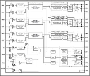
The device 6ED family – 2 nd generation is a full bridge driver to control power devices like MOS-transistors or IGBTs in 3-phase systems with a maximum blocking voltage of +600V. Based on the used SOI-technology there is an excellent ruggedness on transient voltages. No parasitic thyristor structures are present in the device. Hence, no parasitic latch-up may occur at all temperatures and voltage conditions. The six independent drivers are controlled at the low-side using CMOS resp. LSTTL compatible signals, down to 3.3V logic. The device includes an under-voltage detection unit with hysteresis characteristic and an overcurrent detection. The over-current level is adjusted by choosing the resistor value and the threshold level at pin ITRIP. Both error conditions (under-voltage and over-current) lead to a definite shut down off all six switches. An error signal is provided at the FAULT open drain output pin. The blocking time after over-current can be adjusted with an RC-network at pin RCIN. The input RCIN owns an internal current source of 2.8µA. Therefore, the resistor RRCIN is optional. The typical output current can be given with 165mA for pull-up and 375mA for pull down. Because of system safety reasons a 310 ns interlocking time has been realised.
- Thin-film-SOI-technology
- Maximum blocking voltage +600V
- Separate control circuits for all six drivers
- CMOS and LSTTL compatible input (negative logic)
- Signal interlocking of every phase to prevent cross-conduction
- Detection of over current and under voltage supply
- externally programmable delay for fault clear after over current detection
Technical Attributes
Find Similar Parts
| Description | Value | |
|---|---|---|
| Full | ||
| Non-Inverting | ||
| High and Low Side | ||
| 530 ns | ||
| CMOS|TTL | ||
| CMOS, TTL, TTL | ||
| 45 ns | ||
| 800 ns | ||
| 100 ns | ||
| 100 ns | ||
| 100 ns | ||
| Surface Mount | ||
| 6 | ||
| 6 | ||
| 6 | ||
| 1.8 mA | ||
| -40 to 95 °C | ||
| 95 °C | ||
| -40 °C | ||
| 490 ns | ||
| Wafer | ||
| 0.42 A | ||
| IGBT, MOSFET, Mosfet | ||
| 0 | ||
| Industrial | ||
| 375 mA | ||
| 165 mA | ||
| WAFER | ||
| 17.5 V | ||
| 13 V |
ECCN / UNSPSC / COO
| Description | Value |
|---|---|
| Country of Origin: | RECOVERY FEE |
| ECCN: | EAR99 |
| HTSN: | 8542390050 |
| Schedule B: | 8542390060 |