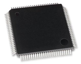
GS88136CGT-200IV
SRAM Chip Sync Single 1.8V/2.5V 9M-Bit 256K x 36 6.5ns/3ns 100-Pin TQFP Tray
- RoHS 10 Compliant
- Tariff Charges
The GS88136C(T/D) is a 9,437,184-bit high performance synchronous SRAM with a 2- bit burst address counter. Although of a type originally developed for Level 2 Cache applications supporting high performance CPUs, the device now finds application in synchronous SRAM applications, ranging from DSP main store to networking chip set support.
- IEEE 1149.1 JTAG-compatible Boundary Scan
- 2.5 V or 3.3 V +10%/–10% core power supply
- 2.5 V or 3.3 V I/O supply
- LBO pin for Linear or Interleaved Burst mode
- Internal input resistors on mode pins allow floating mode pins
- Byte Write (BW) and/or Global Write (GW) operation
- Internal self-timed write cycle
- Automatic power-down for portable applications
- JEDEC-standard 100-lead TQFP and 165-bump BGA packages
- RoHS-compliant 100-lead TQFP and 165-bump BGA packages available
Technical Attributes
Find Similar Parts
| Description | Value | |
|---|---|---|
| 18 Bit | ||
| Flow-Through|Pipelined | ||
| 200 MHz | ||
| SDR | ||
| 9 Mbit | ||
| Matte Tin | ||
| 260 | ||
| 145@Flow-Through|170@Pipelined mA | ||
| 2, 2.7 V | ||
| 6.5@Flow-Through|3@Pipelined ns | ||
| 9 Mbit | ||
| 1.7, 2.3 V | ||
| Surface Mount | ||
| MSL 3 - 168 hours | ||
| 100 | ||
| 36 Bit | ||
| 36 Bit | ||
| 1 | ||
| 256 kWords | ||
| -40 to 85 °C | ||
| 85 °C | ||
| -40 °C | ||
| 100TQFP | ||
| 100 | ||
| 20 x 14 x 1.4 mm | ||
| No | ||
| Industrial | ||
| Synchronous SRAM | ||
| TQFP | ||
| 2, 2.7 V | ||
| 1.7, 2.3 V | ||
| 1.8, 2.5 V | ||
| Synchronous | ||
| 1.8, 2.5 V |
ECCN / UNSPSC / COO
| Description | Value |
|---|---|
| Country of Origin: | RECOVERY FEE |
| ECCN: | 3A991.B.2.B |
| HTSN: | 8542320041 |
| Schedule B: | 8542320040 |
